Abstract: This paper introduces a digital stopwatch design method based on FPGA. Use VHDL hardware description language, use EDA simulation tools such as ModelSim. The design has the advantages of less peripheral circuits, high integration, and high reliability. Finally, the experimental results show that the digital stopwatch has accurate timing and the input signal can accurately control the stopwatch operation. The top-down modular design method adopted by the system is also very useful for other complex system designs.
As the cornerstone of today's information age, digital integrated circuits are not only widely used in the production fields of information processing, industrial control, etc., but also everywhere in people's daily life, which has greatly changed people's way of life. Faced with such a huge market, the design cycle of digital integrated circuits is required to be as short as possible, and the experimental cost is as low as possible. It is better to verify the accuracy and feasibility of the design directly in the laboratory. Thus, a field programmable gate array FPGA has emerged. . For chip design, the ease of use of FPGAs not only makes the design simpler and faster, but also saves the huge cost of repeated tape verification. For some small-volume applications, you can even use FPGA directly, no need to order a special digital chip.
This paper focuses on a digital stopwatch design method based on FPGA using VHDL hardware description language. In the design process, the VHDL-based EDA tool ModelSim is used to simulate and verify each module, and the complete source program and simulation results are given.
1 Overall functional structure designA complete digital stopwatch should have timing, corresponding control, and timing results display. The overall functional structure is shown in Figure 1. The black wireframe is the counting module, the enabling conversion module and the display decoding module. The left side is the input control signal, and the right side is the digital display tube showing the timing result. The reading is displayed by the six-digit BCD seven-segment digital tube. The display format is shown in Figure 2. The timing range is: 1 hour with an accuracy of 0.01s.
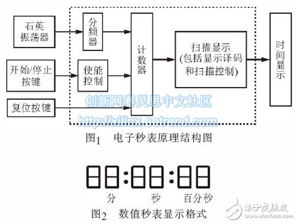
The input clock signal is provided by a 32MHz quartz crystal oscillator. Considering that the design specification requires a stopwatch accuracy of 0.01 seconds, the clock input of the count pulse should be a pulse with a frequency of 100Hz, so first design a 320000 divider, the output of the divider. It can be used as the input of the counter; secondly, the design of the counting module should comprehensively consider the timing range (1 hour) and display output (6-bit output) of the stopwatch. Two of the 6-bit outputs are hexadecimal output, and the remaining four digits are decimal outputs. Therefore, it can be realized by designing 4 modulo 10 counters and 2 modulo 6 counters, wherein the lower bit carry output is the high count input terminal.
The control module should include start timing/stop timing, reset two buttons, that is, the enable and clear terminals that are often used in circuit design. These two control ports can be reset directly by the clearing and history of the counter. Start timing/stop timing; however, the peripheral enable input needs to pass through the enable conversion circuit before it can be changed to the enable control signal available to the counter. Therefore, a signal conversion module needs to be designed between the input enable signal and the counter enable input.
The module that displays the counting result is simpler to implement. It only needs to connect the six-digit counting result to the output through the seven-segment decoding circuit to illuminate the digital tube. Without the timing control, the combination logic circuit can be directly realized. The digital tube display can use a scan display to scan a multiplexer with a signal with a frequency of 1 kHz to achieve a scan output of the counted results of six bits that have been latched.
2 each functional module design 2.1 Divider Module The function of the frequency divider is to provide standard clock control signals to accurately control the opening and closing of the counter. The standard signal provided is 32MHz. According to the design accuracy of 0.01s, the output signal is 100Hz, so the frequency divider is implemented. The function is divided by 320000, specific
VHDL source program:
Process (clk)
Begin
If (clk'event and clk='1') then
If (q=159999) then
q<=0;
Count_temp<=not count_temp;
Else
q<=q+1;
End if;
End if;
End process;
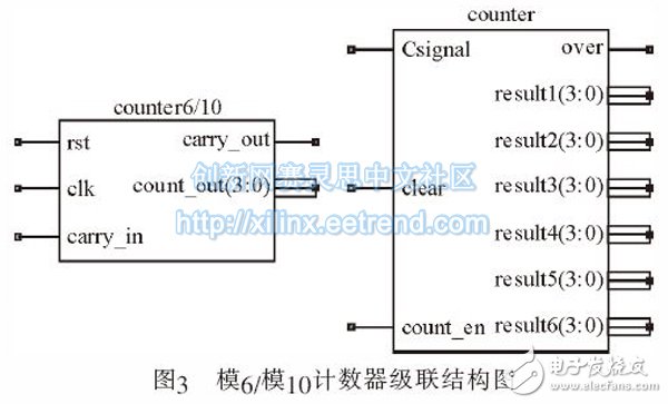
2.2 Counting module The counter should realize the maximum counting value of 59 minutes 59 seconds 99, and for the convenience of digital tube display, the module must be realized by cascade of counters, that is, first design a modulo 6 counter and a modulo 10 counter respectively. Then, they are cascaded, in which 4 modulo 10 counters and 2 modulo 6 counters are called, which can save resources compared to directly designing the counter of the modulo 100 and the counter of the modulo 60. When the cascade is low, the count carry output is connected to the high count input terminal, as shown in Figure 3. Taking into account the requirements of the control module, each counter has three inputs: clock, enable and clear, two outputs: count output and carry output, using asynchronously enabled asynchronous clear design method, each counter Both the enable and the clear are associated with the peripheral enable and clear terminals.
The source code of the module and the simulation results of the ModelSim simulation are as follows:
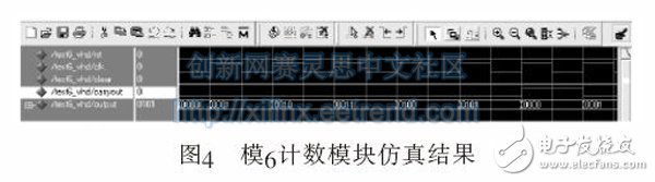
The VHDL source of the modulo 6 counter is as follows:
Process (clear,clk)
Begin
If (clear='1') then
Tmp<=" 0000" ;
Carryout<='0';
Elsif (clk'event and clk='1') then
If (rst='0') then
If (tmp=" 0101") then
Carryout<='1';
Tmp<=" 0000" ;
Else
Tmp<=tmp+1;
Carryout<='0';
End if;
End if;
End if;
The VHDL source of the modulo 10 counter is similar to the modulo 6 counter, which is not given to save space.
Asic Miner Goldshell:Goldshell KD Max,Goldshell KD6,Goldshell KD6-SE,Goldshell KD Lite,Goldshell KD5 Pro,Goldshell KD5,Goldshell KD-BOX Pro,Goldshell KD-BOX,Goldshell KD2
Goldshell Miner is an industry-leading technology company. The company was founded in 2017, we are focusing on high-performance miners and application fields. In the past few years, Goldshell Miner has successfully completed the R&D, mass production, and sales of multiple miners in LTC, CKB, HNS, Sia and other cryptocurrencies. The headquartered is based in Shanghai, Goldshell Miner has offices in Hangzhou, Hong Kong, Singapore,etc. The current R&D personnel account for more than 70% of the company. The core team has more than 10 years of experience in the integrated circuit field. Aiming to become an excellent blockchain computing power provider, and promoting the development of the industry, Goldshell has established an efficient operation system from algorithm research, batch production and delivery, which based on a strong core team and excellent system capabilities. Goldshell continuously improved the computing performance and competitiveness of products, to provide high-performance and high-reliable computing infrastructure and services for the development of digital economy. Especially our household miner-BOX series, allow more customers to join in the market since our product are small, quiet, affordable, and friendly to beginners so that everyone could start mining at home.
Asic Miner Goldshell,Kd Max 40.2Th,Goldshell kda miner,goldshell kd max,goldshell kd6 miner
Shenzhen YLHM Technology Co., Ltd. , https://www.ylhm-tech.com