With leading-edge DSP, FPGA and CPU working at lower and lower supply voltages and consuming larger currents, it is not so easy to choose a PWM controller. Voltages below 1V have become very common, while the intermediate bus voltage remains basically the same, and even increases in some specific applications. The system frequency is also steadily increasing to support smaller inductance and capacitance (L&C) filtering. Last year's 500kHz became 1MHz this year.
In high-voltage applications that require lower output voltages, power supply designers generally rely on modules that increase system cost, or two-stage DC/DC solutions that increase the size and complexity of the solution. This article focuses on the trends affecting the narrow on-time point-of-load (POL) conversion, and compares it with the commonly used current-mode control architecture. The article discusses the hybrid valley current mode (VCM) architecture with adaptive slope compensation, including its use in a new type of 60V synchronous buck controller, which can operate in a wide range of Vin and Vout combination conditions and Provides stable operation under low duty cycle conditions, so direct step-down conversion from 48V to 1V load point can be achieved.
Demand for narrow on-time load point conversion
The step-down converter is the most widely used power supply topology. Recent development trends indicate that the next-generation switching controller must be able to provide stable and efficient work under very small duty cycle conditions. Although the current mode control method has many advantages over the voltage mode control, there are some limitations of its own that depend on the application requirements, especially in terms of duty cycle limitations.
Generally speaking, power supply systems in telecommunications and industrial applications use multi-level conversion circuits. There is also a continuous power supply system in which the input voltage at the point of load changes from 3.3V to 5V and then to 12V over time. As power requirements increase, the use of 12V power rails is now commonplace, while the use of 3.3V power rails is becoming less and less. This trend toward higher input voltages is partly due to higher currents causing I2R (current-to-resistance) power losses and related problems in low-voltage circuits.
Recently, this trend is also moving towards higher voltages, such as 24V~42V for industrial applications and 48V for telecommunications. Continuous technological progress has made it possible to control narrow pulses. At the same time, new research shows that higher input voltage can achieve higher overall efficiency, lower system cost, and improve system reliability by reducing the temperature of the distribution path.
Another factor required to drive PWM narrow pulses is the need for higher switching frequencies, which will result in higher power densities. It is already common for power supplies to operate at a switching frequency of 1MHz. In fact, in automotive infotainment applications, in order to avoid the AM frequency band, this switching frequency needs to exceed 1.8MHz. To achieve a 12V to 1V power conversion at 1MHz, a 83ns pulse is still needed.
Limitations of low duty cycle operation
An ideal buck converter can generate any voltage lower than Vin, even to 0V. However, there are many limitations in practical applications, such as reference voltage, internal or external circuit losses, and more importantly, a modulator used to generate control signals Types of. For a particular input voltage, the reference voltage is the most obvious limiting factor preventing the controller from covering the entire range from 0% to 100%. The most obvious is the reference voltage:

This formula shows that the output can be adjusted below the Vref voltage. The second major limiting factor in obtaining the minimum Vout is the minimum on-time of the controller. For a given input voltage (Vin), the minimum Vout can be expressed as:

For a given switching frequency (Fs), the on-time of the upper MOSFET is equal to:

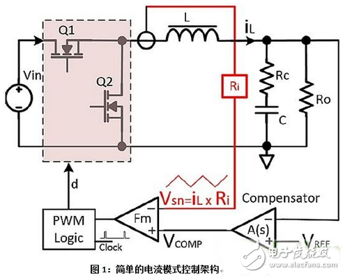
Most of the control methods used by the controller are used to drive the minimum on-time it can control. Some intentional delays inside the gate drive circuit, such as blanking time, will also affect the minimum on-time. In a typical current mode PWM controller, the size of the PWM pulse depends on the output of the error amplifier and the inductor current signal, as shown in Figure 1. The current loop detects the inductor current signal and compares it with the VCOMP reference value. The comparison result is used to modulate the PWM pulse width. Since the current loop forces the peak or valley current of the inductor to follow the voltage error amplifier output, the inductor does not appear in the voltage control loop. For the voltage loop, the two-pole LC filter will become a single-capacitor pole structure. Simple type 2 compensation is sufficient to stabilize the voltage loop.
Modulator suitable for narrow on-time operation
Peak current mode control is one of the most commonly used architectures. Although it is well understood and can provide a reliable control technique with many advantages, it will present significant shortcomings when a narrow on-time operation is required. In peak current mode, the inductor current information is detected on the upper MOSFET. Figure 2 shows the typical current waveforms related to the PWM signal in the upper and lower MOSFETs. The turn-on event of the upper MOSFET will cause significant ringing due to different parasitic parameters inside and outside the MOSFET in the turn-on loop. This kind of ringing will send an error signal to the control circuit, and erroneously terminate the PWM signal.
To solve this problem, the peak current mode switching controller uses a blanking time to ignore this initial ringing before detecting the inductor current. The general blanking time is 150ns to 250ns. This blanking time requirement does not allow the peak current mode controller to regulate very narrow on-time power conversion. At a frequency of 600kHz, even a 12V to 1V power conversion is difficult to adjust. This frequency is equivalent to a minimum on-time of less than 140ns.
Valley current mode control
Another method is valley current mode control, which can easily overcome the defect of blanking time under peak current mode control. Under valley current mode control, the detection of the inductor current signal is carried out during the turn-off period of the upper MOSFET, thereby avoiding ringing of the upper MOSFET. This method solves the problem of controlling very narrow on-time PWM pulses. However, the valley current mode also has some limitations of its own.
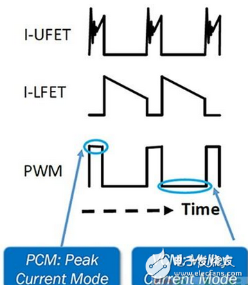
Figure 2: The buck converter waveform shows the signal detection position in the current-mode control architecture.
There are two main problems with valley current mode control, namely sub-harmonic oscillation and poor linear regulation. Sub-harmonic oscillation is a common problem in any current mode control scheme. It also occurs in peak current mode control, but it always occurs when the duty cycle exceeds 50%. For valley current mode, the situation is just the opposite.
The sub-harmonic oscillation in the current mode controller (whether it is peak mode or valley mode) can be avoided by slope compensation. However, fixed slope compensation cannot cope with all duty cycles and inductances. If the duty cycle is far from the set value used in the slope compensation design, sub-harmonic oscillation problems will still occur.
Peak current mode control
Another method is emulation peak current mode control, which is a variant of peak current mode, which can avoid the blanking time limit. By measuring the valley current information on the low-side MOSFET, this method can overcome the ringing of the upper-side MOSFET. This valley current information can then be used to simulate the inductance overshoot to obtain peak current information.
Like the peak current mode control, the simulated peak current mode also has the problem of sub-harmonic oscillation, which requires slope compensation. This slope compensation is derived from the simulated peak current signal. Although the simulated peak current mode design has the advantages of both the bee current mode and the valley current mode control method, it also has disadvantages, mainly because of the lack of inductance information in the control loop.
Combines the advantages of both modes
The valley current mode with adaptive slope compensation function is a method to overcome the shortcomings of traditional valley current mode control. The optimized adaptive slope compensation circuit can prevent sub-harmonic oscillation under all duty cycle conditions. The inherent ability of this adaptive compensation and low duty cycle operation allows the controller with this architecture to work at a very high switching frequency.
Intersil's ISL8117 step-down controller uses a valley current mode control, which has low-side MOSFSET Rdson, valley current detection and adaptive slope compensation. As shown in Figure 3, the ramp signal of the ISL8117 can adapt to the applied input voltage, thereby effectively improving the line regulation rate. Its unique valley current mode implementation and optimized slope compensation function overcome the shortcomings of traditional valley current mode controllers. The unique control technology of ISL8117 makes it support a wide range of input and output voltages. In fact, ISL8117 is a hybrid method of voltage mode control and current mode control, and has the advantages of two modulation architectures at the same time.
The ISL8117 can work at any voltage in the range of 4.5V to 60V, and its output can be adjusted from 0.6V to 54V. It has an adjustable frequency range from 100kHz to 2000kHz and can produce a minimum on-time of 40ns (typical value). With the shortest on-time of 40ns, the controller can generate 1V output from the 12V bus at a frequency of 1.5MHz. It can also generate a 1V supply from a 48V power supply at a lower frequency. Figure 4 shows the instantaneous transition from a stable 48V to 1.2V. In systems that are susceptible to noise at a specific switching frequency, the ISL8117 can be synchronized to any external frequency source to reduce radiated system noise and beat noise.
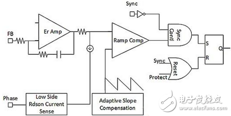
Figure 3: Internal control block diagram of ISL8117. 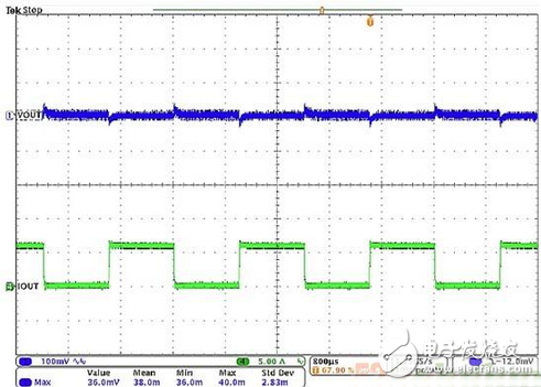
Figure 4: Transient response from OA to 6A and 6A to OA produced by a stable 48v to 1.2v converter.
With this synchronous step-down controller, engineers can design a complete DC/DC conversion solution with only 10 components including MOSFETs and passive components, and can achieve 98% conversion efficiency and 1.5% conversion efficiency. Output voltage accuracy. As shown in Figure 5, the low pin count and layout-friendly pin structure of the ISL8117 can also minimize the number of crossover traces and further improve power supply performance.
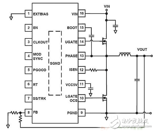
Figure 5: Typical application of ISL8117.
Summary of this article
Each modulation control mode has its own limitations, but recent innovations, such as the ISL8117 60V buck controller with hybrid valley current mode and adaptive slope compensation, can be used to design power supplies more flexibly and conveniently solution. ISL8117 can help system designers remove intermediate conversion stage circuits, use a smaller volume to achieve higher efficiency, while reducing system costs and improving product reliability.
MODULE PHOTOVOLTAIC
Wuxi Shengda Yukun Energy Development co.,Ltd , https://www.xlite-solarlight.com