Abstract: In the engineering practice based on FPGA chip, FPGA is often required to communicate with host computer or other processors. For this purpose, a UART interface module for short-range communication is designed. The program of the module is written in VHDL language. The core sending and receiving sub-modules of the module are designed by finite state machine. The design ideas and methods of each sub-module are detailed, and their simulation timing diagrams are given. After the comprehensive implementation, the program is downloaded to the FPGA chip and the operation is correct. It is also stable and reliable after long-term transmission and reception tests. Relative to the fixed parameter design, the baud rate, data bit width, stop bit width, check bit enable and check mode selection of the UART can be set online, which provides a reliable way for FPGA to communicate with other devices. Has a strong practical value.
0 IntroductionAlthough the Universal Asynchronous Receiver (UART) has been around since the 1970s, it is still a widely used serial communication interface because of its simplicity and reliability. A variety of microprocessors, whether it is a microcontroller, or DSP, ARM, UART are basic peripheral modules. In many cases, such as system monitoring and data acquisition, serial communication [1-3] is used, and even multiple serial ports are used, such as developing serial port servers [4-6]. At this time, special chips are usually used, such as 16C554, VK3224 and other extended serial ports. The dedicated chip is simple to use, but lacks flexibility. At the same time, the number of serial ports integrated by the dedicated chip is limited, and sometimes multiple chips are needed to meet the requirements [5], which increases the complexity of the system and reduces the reliability.
As a programmable chip, FPGA (field programmable gate array) is rich in resources and high in work efficiency. It is often used for high-speed data acquisition and high-speed parallel execution of algorithms [7-8]. Users can design personalized high-performance circuit modules through hardware description language or circuit schematics, which has the advantages of flexible design and convenient upgrade.
In FPGA-based engineering practice, it is often required to communicate with serial devices, but there is no related IP core in Xilinx's existing development environment ISE. At present, there are examples of using FPGA to design UART [9-13], but some parameters are fixed and lack of versatility. This paper designs and implements a UART interface module with parameters that can be configured online, which provides a reliable way for FPGA to communicate with other devices.
1 Introduction to UART Serial CommunicationThe standard RS232 interface often uses a DB-9 connector, which has 2 data lines, 6 control lines, and 1 signal ground. The UART designed in this paper conforms to the RS232 serial communication standard, but in practice, many control signals in the RS232 standard are used less. Therefore, the UART in the text uses only three of the signal lines, namely TXD, RXD and signal ground, which is also a lot. The signal line used by the microprocessor UART module.
The UART is an asynchronous communication interface, and both parties must agree on the baud rate. A series of standard baud rates are specified internationally, such as 9 600 b/s, 19 200 b/s, 115 200 b/s, etc. Each data frame of the UART is composed of a start bit (1 bit), a data bit (5-8 bits), a parity bit (optional 1 bit), and a stop bit (1 to 2 bits). The data bit portion is transmitted from the lowest bit first; the parity bit is calculated for the data portion and the check bit in the 1-frame data, so that the number of '1's satisfies an odd number or an even number. When the UART is idle, the transceiver pins RXD and TXD are both high. Once the data needs to be transmitted, the low level is first output to the TXD pin as a start bit, indicating the start of 1 frame of data. When receiving data, detecting the start bit will initiate a data reception process.
2 system designThe UART communication interface designed in this paper is mainly composed of baud rate generation module, transmission module, receiving module and microprocessor interface module. Each module is expressed in VHDL language, and the signal connection between the modules is realized by the component instantiation statement in the top-level file.
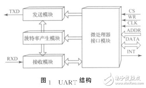
The block diagram of the entire design is shown in Figure 1. The main functions of the UART communication module designed and implemented are as follows:
1) The transmission and reception of serial data is realized.
2) The stop bit can be set (1 bit or 2 bits).
4) The baud rate is configurable. The standard baud rate series can be set from 9 600 to 115 200 b/s, and also supports a custom baud rate.
5) Designed a microprocessor interface, through the interface to access the UART internal registers, configure UART parameters, read and write data.
The UART communication interface consists of two data buffer registers (TxHolder and RxHolder), three control registers (UartCon, UartBaud, and UartIntEn), and three status registers (UartState, UartError, UartIntPend). Considering the need to update the UART parameters online, UartCon and UartBaud are designed as double buffer registers. The first level buffer is used to store the configuration data written by the external processor, and the second level buffer is used to set the UART core. When the UART core is idle, the second-level buffer content is updated to the first-level buffer content to prevent damage to the data in the transceiver.
3 UART module designThe design ideas and methods of each UART module are described in detail below, and the behavior simulation timing diagram of the main module is given.
3.1 Baud Rate Generation ModuleThe function of the baud rate generation module is to generate the clock signal required for UART operation, and its frequency is set to 16 times the actual baud rate. The baud rate generation module is essentially a counter that can be preset with an initial value. When the count reaches the preset value, it outputs a high level, and the remaining values ​​output a low level.
3.2 Sending moduleThe sending module serially transmits the parallel data in the TxHolder according to the user setting, and its core is a finite state machine, and its state transition is as shown in FIG. 2 .
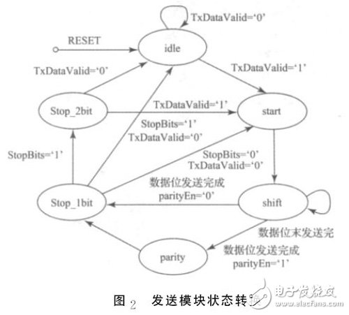
1) Idle state After the system power-on reset, the transmitting state machine enters this state. If data is not written to the transmit buffer, then TxDataValid is low, indicating that the transmit buffer is empty, the state machine is always waiting in this state loop, and the TXD pin outputs a high level.
2) Start state Once data is written to the transmit buffer TxHolder, TxDataValid goes high. The state machine switches from the Idle state to the Start state, TXD outputs a low level, and outputs a start bit.
3) Shift state After the 1-bit baud time has elapsed, the state machine unconditionally transitions to the Shift state. Even if the shift register can be sent, the parallel data is shifted to the right by bit, and the parallel-to-serial conversion is performed and output to the TXD. When the number of output data reaches the data bit width set by Databit, it will switch to Parity or Stop_1bt state, otherwise it will still switch to this state.
4) Parity state If the data bit part is transmitted and the parity enable bit ParityEn='1', then it transitions to this state. In this state, the check digit is transmitted based on the transmitted data and the selected check mode.
5) The Stop_1bit state first switches to the Stop_1bit state regardless of whether the stop bit is 1 bit or 2 bits, and first outputs 1 stop bit. When the next state is switched from this state, there are many cases in the secondary state. If the stop bit is set to '1', the second stop bit is selected, the second state is stop_2bit; if the stopbit is '0' and the transmit buffer is empty, the secondary state is converted to the idle state, otherwise the transition to the start state starts new. A round of data transmission.
6) If the Stop_2bit status selects 2 stop bits, it will enter this state. After 1 baud time, according to the TxDataValid state, enter the Idle state to stand by, or enter the Start state to start a new round of data transmission.
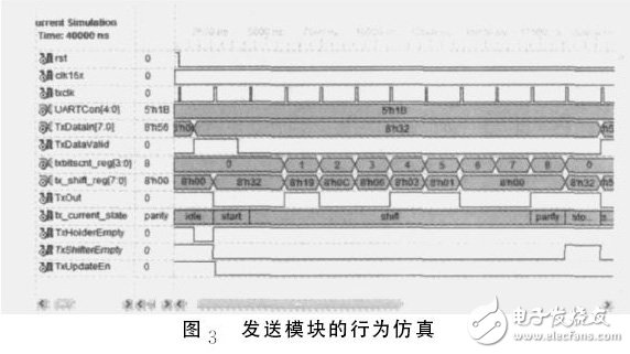
The behavior simulation timing diagram of the sending module is shown in Figure 3. Its UART parameters are set to even parity, 8-bit data bits and 1-bit stop bits. Txclk is the transmit sample clock signal. On the rising edge of the signal, the transmit state machine state is inverted and the data is sent to the TxOut (TXD) pin. In the figure, the data output by TxOut is “00100110011â€. After the start bit, check bit and stop bit are removed, the data to be transmitted is 0x32. It can be seen from the timing diagram of the transmission module obtained by the simulation that the simulation results of the signals of the module are correct.
Stainless Steel Precision Pipe
Stainless Steel Precision Pipe,High Precision Ss Pipe,Stainless Steel Precision Tube,High Performance Precision Ss Pipe
ShenZhen Haofa Metal Precision Parts Technology Co., Ltd. , https://www.haofametals.com