Linux is an open source, networked operating system that is stable, efficient, and freely configurable. The use of the Linux operating system as a development platform not only has a free advantage compared with the use of VxWorks and Windows as a development platform, but also has an extremely important significance for developing core technologies and improving information security, and is a direction of independent research and development. With the rapid development of weather radars in China, weather radars are becoming more and more widely used in civil and military fields. At present, the high-speed data acquisition and transmission functions of weather radar are mostly developed based on the Windows platform, and the conversion from Windows platform to Linux platform is of great significance for developing China's independent intellectual property meteorological software core technology and improving information security. This paper is based on the Linux operating system (2.6.23 kernel), which realizes high-speed data acquisition and processing of weather radar. It has reference value for the weather radar system from Windows platform to Linux platform.
1 Data acquisition system analysis1.1 Working principle
The weather radar high-speed data acquisition system consists of I/Q data acquisition, FIFO buffer, FPGA control module and PCI bus chip PLX9054. The system structure block diagram is shown in Figure 1.
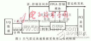
The core part is the FPGA control module, which mainly implements 4 functions: (1) adjust the frequency of the AD sampling clock according to the radar range and distance resolution; (2) control the AD two-way sampling data to be written into the FIFO buffer and the DMA transmission from the FIFO Continuous reading of data; (3) Control interaction with PCI bus control chip PLX9054, realize local bus read/write control, address decoding and interrupt triggering; (4) Data interaction with PLX9054, use FPGA internal RAM to save and control weather The commands and data of the radar transmitter and receiver work to complete the control of the radar work.
The I/Q data acquisition and output data speed is 2.4 Mb/s (I and Q data are each 24 bits), which are controlled by the FPGA and combined into the FIFO buffer. The FIFO buffer is a 32-bit data buffer with a depth of 16 KB, and the effective bit is 24 bits. The interface with the computer bus uses a 32-bit PCI bus interface chip PLX9054, through which the PC performs data interaction with the data acquisition system.
1.2 PC and acquisition system data access
1.2.1 Local Address Assignment
The data access of the PC and weather radar high-speed data acquisition system is realized by the PCI bus chip PLX9054, and the access target is FIFO buffer and FPGA on-chip RAM. Different local addresses are allocated to the FIFO buffer and the FPGA on-chip RAM, and the target to be accessed is determined by decoding the local address bus. The FIFO data is continuously read by DMA transmission. The maximum length of each transmission is 8 KB. Therefore, the 32-bit local address range of the FIFO space is set to 0x20000000 to 0x2000FFFF, and the mapping space is the PCI address space bar2.
The on-chip RAM has a bit width of 32 bits and a local address range of 0x40000000 to 0x400FFFFF. The mapping space is the PCI address space bar3.
1.2.2 Data Access Method
The FIFO buffer is a programmable FIFO that is controlled by the FPGA based on the on-chip stored radar parameters. When the data in the FIFO reaches the set size, the PCIPLX9054 is triggered to trigger a PCI interrupt, through which the driver is requested to initiate a DMA transfer. The driver responds to the interrupt and sets the DMA register of PCIPLX9054 to initiate DMA transfer from the local bus to the PCI bus to complete the transfer of FIFO data to the PC.
The on-chip RAM of the FPGA uses PCI address mapping to perform data read and write access using the IO operation mode.
2 Linux program implementationThe weather radar high-speed data acquisition system is based on the Linux 2.6 kernel platform program and consists of a PCI bus-based device driver, data acquisition and processing program.
2.1 device driver implementation
The function of the device driver is to realize the data interaction between the PC and the acquisition board through the control of the PCI bus control chip PLX9054 under the Linux 2.6 system platform, realizing the real-time reception of the radar acquisition data and the control of the radar working state. From the functional structure, the device driver is mainly composed of three parts: device loading and initialization, interface function provided to the user layer, interrupt and DMA data transmission.
2.1.1 Equipment loading and unloading
Device loading and unloading is the device driver installation and uninstallation in Windows systems. In Linux 2.6, the loading and unloading is mainly realized by calling the PCI bus driver registration function pci_register_drive and the logout function pci_unregister_driver provided by the system. The registered driver data structure is as follows:
staTIc struct pci_driver plx9054_pci_driver = {
.name = 'pci9054',
.id_table = plx9054_pci_tbl,
.probe = plx9054_probe,
.remove = plx9054_remove,
};
When the system boots, after the high-speed data acquisition system is powered on, the on-board PCI bus firmware configures the PLX9054 device by default, allocating resources for each address area of ​​the device. The load function is declared in the driver with module_init, the initialization of the device is performed, the PCI bus driver registration function is called, the PCI device PLX9054 is detected and identified according to the information defined by the id_table, the PCI bus registration of the PLX9054 device driver is completed, and then the driver registered with the driver is called. Function, complete PLX9054 device enable, PCI address space mapping, PLX9054 device data structure initialization, device registration (registered as a character device) and other operations. The unload function is declared with the module_exit, which is the reverse process of loading. By calling the PCI bus to drive the unload function, then calling the registered remove function, unregistering the device and the PCI address space mapping, releasing the data structure space allocated to the device, etc., to complete the system resource release. .
2.1.2 Device Interface Functions
The device interface function provides the user with different functional interfaces for interacting with the device, and mainly performs functions such as reading, writing, and device control access of the user and the device, and the data structure is designed as follows:
staTIc const struct file_operaTIons plx9054_fops = {
.owner = THIS_MODULE,
.open = plx9054_open, /*Open device*/
.release = plx9054_close, /*release device*/
.ioctl = plx9054_ioctl, /*IO operation*/
.read = plx9054_read, /*read device*/
};
During the device loading process, the data structure is connected to the device as a parameter registered by the device, so that the user can access the associated device interface function in the system call.
Fiber Optic Box,Fiber Optics Box,Fiber Optic Boxes,Fiber Optic Junction Box
Cixi Dani Plastic Products Co.,Ltd , https://www.dani-fiber-optic.com