Abstract: The basic principle of direct digital frequency synthesis (DDS) is introduced. Based on Xilinx FPGA, a system scheme for generating radar signals such as continuous wave, repetitive jitter, frequency agility, chirp and two-phase coding is designed. The experimental results show that the design is flexible and has good performance and has broad application prospects. Radar sources are a core part of modern radar systems. With the development of electronic information technology, radar systems are increasingly demanding radar signal sources [1].
Based on the idea of ​​software radio and the basic principle of direct digital frequency synthesis, this paper uses Xilinx's Virtex-5 series XC5VLX70T FPGA to realize phase accumulation, waveform lookup table, PCI9054 interface design and digital/analog conversion chip AD9737. Register configuration and some logic control. The Verilog HDL hardware description language is used in the ISE development environment to complete the entire process of hardware design, simulation, synthesis, and testing, and can be flexibly modified according to actual needs. This method not only improves the design efficiency, but also makes the system have the characteristics of flexible design, simple implementation and stable performance. The generated radar signal has the advantages of high resolution and continuous phase adjustment, which can meet the requirements of modern radar systems.
The block diagram of DDS is shown in Figure 1.
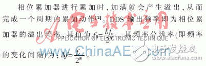
It is mainly composed of a reference frequency source, a phase accumulator, a waveform memory (ROM), a digital-to-analog converter (DAC), and a low-pass filter. The essence of DDS is to use the sampling theorem to generate waveforms by phase-to-ROM look-up table. The core part of the DDS is the phase accumulator, which is an N-bit full adder that accumulates the input frequency control words.

Let the reference clock be fc, the frequency control word be k, the phase accumulator word length be N, and the waveform memory (ROM) store 2N data (one cycle). The working process: under the driving of the reference clock fc, the phase accumulator performs the accumulating operation with the step length k, obtains the phase-to-ROM addressing, and outputs the corresponding amplitude code, and then obtains the output waveform through the digital-to-analog converter [1] -4].
The system block diagram of the radar-based IF signal source based on FPGA is shown in Figure 2. The system is mainly composed of CPCI single board computer, PCI9054 chip, Xilinx FPGA, digital/analog converter AD9737, low pass filter and clock circuit. When the system works, the human-computer interaction control is completed by the CPCI computer, communicates with the FPGA through the PCI9054 bus interface, and writes the signal parameters; the DDS simulation is implemented in the FPGA, and the corresponding digital waveform is generated according to the set parameters; The conversion chip AD9737 converts the digital signal into an analog signal, and outputs a radar intermediate frequency signal through a low-pass filter.
2.1 System signal processing flow
As shown in FIG. 3, through the computer software interface interface, the user inputs signal carrier frequency, output power, signal type, pulse repetition time (PRT), pulse width (PW), and other signal waveform data and characteristic parameters to the single board computer. And through the PCI9054 bus to send to the various working modules of the system.
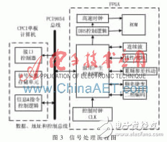
The control software sets the parameters of each module in the system according to the operation instruction issued by the user, and uses the information control word, the command control word and the signal setting parameter, and performs process control in the process of signal generation. After completing the task of data transfer, the individual waveform generators and DDS are initialized by the control logic. Each waveform generator unit sets a relevant calculation variable in the waveform generation process according to the input signal data parameter. After the initialization is completed, the current logic information is returned to the single board computer by the control logic. After the initialization task is completed, the control logic controls the generation process of each signal waveform generator according to the content of the message control word, and then the radar digital signal is generated by the DDS, and is converted into an analog signal by the AD9737 and output.
The requirements of various indicators of the system: signal frequency range: 0~400 MHz; frequency resolution: ≤10 kHz; pulse width: 50 ns~400? 滋s; pulse repetition interval: 4? s~10 ms; AD9737 sampling frequency: 1 Gb/s; ROM storage data: 11 bit offset binary code; output signal type: continuous wave, repetitive jitter, frequency agility, two-phase encoding, chirp.
2.2 DDS module design
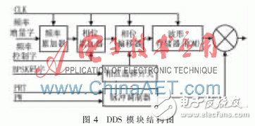
The DDS module is implemented by FPGA, and its structure is as shown in FIG. 4, and is composed of a frequency accumulator, a phase accumulator, a phase offset accumulator, a waveform memory (ROM), and a phase selection switch. Wherein, the frequency accumulator is used to control the frequency increment when generating the chirp signal; the phase accumulator is the same as the ordinary DDS, the input frequency control word, the output data is the phase of the synthesized signal, and the overflow frequency of the phase accumulator is the DDS output signal. Frequency [3]; phase offset accumulator is used to generate BPSK signal, the phase offset has 0 and ?; use the data generated in the previous part as the phase sampling address of the waveform memory (ROM), so that the memory can be stored The waveform sample values ​​in the ROM are detected by the lookup table to complete the phase-to-amplitude conversion; the pulse repetition time (PRT) and pulse width (PW) signals are input to the pulse modulator, and the output signal is multiplied by the ROM output waveform to generate The re-frequency modulated signal.
2.3 ROM module design and optimization
Xilinx's Virtex-5 series FPGAs provide the IP core of the Block ROM. The memory initialization is performed using the memory initialization (.coe). After the power is turned on, the content is kept unchanged, that is, the ROM function is realized.
First, the quantization bit width of the stored sine wave is determined, and the D/A chip AD9737 selected by the scheme provides an 11 bit quantization bit width. In order to ensure the quantization accuracy of D/A, the data stored in the ROM memory should correspond to the D/A chip quantization bit width on the premise of resources.
The block memory resources in the FPGA chip are valuable, and thus the ROM capacity is required. According to the parity symmetry and periodicity of the sine wave, only one quarter of the sinusoidal data can be stored. At this time, the first two bits of the phase accumulator output phase code are quadrant information, "00" is the first quadrant, "01" is the second quadrant, "10" is the third quadrant, and "11" is the fourth quadrant. The first digit in the phase code is the polarity identifier, "0" is positive polarity, and "1" is negative polarity [1]. 2.4 parallel/string conversion
The program directly generates the radar IF signal, the output analog signal frequency is up to 400 MHz, and the AD sampling frequency is 1 GHz. The Virtex-5 series XC5VLX70T FPGA has a maximum operating frequency of 550 MHz [1]. According to the idea of ​​parallel/serial conversion, four parallel ROM modules [5] are designed using the area exchange speed, as shown in Figure 5.
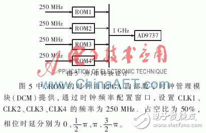
The digital-to-analog conversion chip has a clock of 1 GHz and is provided by the Rocket I/O hard core inside the FPGA. It uses CML, CDR, line coding and pre-emphasis techniques to greatly reduce clock distortion, with a maximum rate of 10 Gb/s or more [2]. When set, the input is placed in an 8-bit "10101010" sequence with a code rate of 2 Gb/s, which gives an accurate clock of 1 GHz.
3 Radar system signal generation method and simulation The principle of generating continuous wave signals is relatively simple and will not be described here. The following describes the implementation of radar signals such as fixed-frequency, re-frequency jitter, chirp, frequency and two-phase coding, and gives the simulation results of ModelSim [6].
(1) Fixed re-frequency radar signal and re-frequency jitter radar signal
The fixed re-frequency radar signal is based on the continuous wave signal, adding the re-frequency modulation information, inputting the PRT and PW parameters to the pulse modulator to generate the pulse signal, and then multiplying by the continuous wave to obtain [7]. Figure 6 shows the fixed re-frequency radar signal.
Compared with the fixed re-frequency radar signal, the re-frequency jitter radar signal has a random change in its PRI. Here, a pseudo-random M-sequence is used to implement PRI jitter from +12.5% ​​to -12.5% ​​using a 5-bit shift register. The schematic diagram of the pseudo random noise code generation is shown in Fig. 7.
(2) Linear frequency modulated radar signal
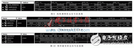
There is a linear relationship between the time and frequency of the LFM signal [7]. Add a frequency accumulator in front of the ordinary DDS, input the frequency increment word, change the frequency control word, and thus change the frequency of the output signal. The frequency increment word set by this design is a fixed value, and the output signal is a chirp signal, as shown in FIG. Of course, if the frequency increment is a varying value, the output signal is a non-linear FM signal.
(3) Phase coded radar signal Â
A phase shifter and phase switch are added after the DDS module. The phase offset has two types, 0 and π. Input the bpsk codeword to the phase switch. When the symbol is 0, the phase offset of π is generated. When the symbol is 1, the phase offset of 0 is generated, that is, the phase remains unchanged. Figure 9 shows the simulation results of a 4-bit two-phase coded radar signal with a codeword of 1100.
(4) Frequency agile radar signal
Compared with the conventional radar signal, the frequency agile signal changes its frequency, and other parameters remain unchanged [7]. The scheme implements the pulse group agility based on the state machine, and controls the change of the frequency control word by using the state change, that is, one frequency control word in one pulse period and another frequency control word in another group pulse period. Figure 10 shows two sets of frequency agile radar signals.
Based on FPGA, this paper improves on the basis of DDS principle. In ISE software environment, using Verilog HDL language programming, the waveforms of continuous wave, heavy frequency staggered jitter, frequency agility, chirp and phase encoding are realized. After the experimental test of Virtex-5 XC5VLX70T chip, the verification scheme is feasible and the effect is good. Compared with the dedicated DDS chip, the design scheme is simpler, lower in cost, shorter in development cycle, and has more types of signals and better waveform quality.
references
[1] Xiang Shengwen. Performance Analysis and Improvement of DDS Radar Signal Source [D]. Xi'an: Xi'an University of Electronic Science and Technology, 2006.
[2] Xu Wenbo, Tian Wei. Practical tutorial for XILINX FPGA development [M]. Beijing: Tsinghua University Press, 2012.
[3] Xiong Peilei, Zhang Jianyun, Liu Chunquan.Application of FPGA in Radar Signal Simulator[J].Microcomputer & Applications,2010,29(6):10-12.
[4] Chen Yajun, Chen Longdao. Design of signal generator based on Verilog HDL[J]. Electronic Devices, 2011, 34(5): 525-528.
[5] Wang Mang, Lu Weixiang. Broadband Signal Generation Based on High Speed ​​D/A AD9739[J].Radar and Confrontation,2011,31(4):55-58.
[6] Xia Yuwen. Verilog Digital System Design Tutorial (Second Edition) [M]. Beijing: Beijing University of Aeronautics and Astronautics Press, 2008.
[7] Zhang Mingyou, Wang Xuegang. Radar System [M]. Beijing: Publishing House of Electronics Industry, 2006
Mining is the process of creating a block of transactions to be added to the Ethereum blockchain in Ethereum's now-deprecated proof-of-work architecture.
The word mining originates in the context of the gold analogy for cryptocurrencies. Gold or precious metals are scarce, so are digital tokens, and the only way to increase the total volume in a proof-of-work system is through mining. In proof-of-work Ethereum, the only mode of issuance was via mining. Unlike gold or precious metals however, Ethereum mining was also the way to secure the network by creating, verifying, publishing and propagating blocks in the blockchain.
Mining ether = Securing the Network
Mining is the lifeblood of any proof-of-work blockchain. Ethereum miners - computers running software - used their time and computation power to process transactions and produce blocks prior to the transition to proof-of-stake.
ETH Miner:Antminer E9 2.4Gh/S,Bitmain E9 2.4Gh/S,Bitmain Antminer E9 2.4Gh/S
Eth Miner ,Antminer E9 2.4Gh/S,Bitmain E9 2.4Gh/S,Bitmain Antminer E9 2.4Gh/S
Shenzhen YLHM Technology Co., Ltd. , https://www.hkcryptominer.com