Today, we're going to introduce the basic concept of the digital backend—specifically, the FinFET Grid, which is also known as a design grid. Before diving into this, let's first understand what FinFET technology is and why it's so important in modern chip design.
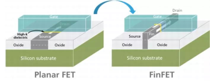
FinFET stands for Fin Field-Effect Transistor. It's a type of advanced CMOS transistor that represents a major breakthrough in semiconductor technology. The term "Fin" comes from the shape of the transistor, which resembles a fin. This three-dimensional structure allows for much better control over the flow of current compared to traditional planar transistors.
One of the key advantages of FinFETs is their ability to reduce gate length significantly. Current FinFETs can have gate lengths under 25 nanometers, with future advancements expected to push this down to around 9 nanometers. To put that into perspective, this is about 1/10,000th the width of a human hair. Such miniaturization enables designers to create powerful computing systems that are incredibly small—potentially as tiny as a fingernail.
In simple terms, FinFET technology creates a new type of 3D multi-gate transistor that dramatically improves processing speed while reducing power consumption. This makes it especially crucial for today’s mobile devices, where energy efficiency is a top priority. FinFETs play a critical role in advancing chip technology to the 16nm and 14nm process nodes, enabling more powerful and efficient chips than ever before.
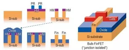
After getting a clear understanding of FinFET technology, let's move on to the FinFET Grid concept. This grid is essential in the design flow and corresponds to the grid unit used in FloFplan for FinFET-based designs.
In a FinFET design, all components—including macros—are aligned to the FinFET Grid. This alignment ensures consistency and precision during the layout process. The grid is defined in the technology LEF file as follows:
PROPERTYDEFINITIONS
LIBRARY LEF58_FINFETSTRING " FINFET PITCH 0.010 OFFSET 0.30 VERTICAL ; " ;
LIBRARY LEF58_FINFET STRING " FINFET PITCH 0.091 OFFSET 0.30 HORIZONTAL ; " ;
END PROPERTYDEFINITIONS
The keywords “VERTICAL†and “HORIZONTAL†correspond to the pitch along the X and Y axes, respectively. These values define how components are placed and spaced within the design.
At first glance, these technical details might seem overwhelming. However, modern back-end tools have made it easier to handle such complex technologies through intuitive software interfaces. This simplification allows engineers to focus on innovation rather than getting lost in the complexity of the underlying design rules.
The touch monitor is a product developed and designed by ourselves. It has been sold for more than 6 years and has exceeded 160,000 units. At present, it is running very well. It mainly customizes different touch technologies, different sizes, different interfaces, connecting cables and power supply parts to meet the needs of guests. We provide customers with the choice of Resistive Touch Screen, Capacitive Touch Screen, infrared Touch Screen and nano Touch Foil , and customize various interfaces for customers, such as: VGA, DVI, HDMI, DP and so on. It is mainly used in banks, hospitals, government units, airports, railway stations, supermarkets, real estate and other places.
Product show:

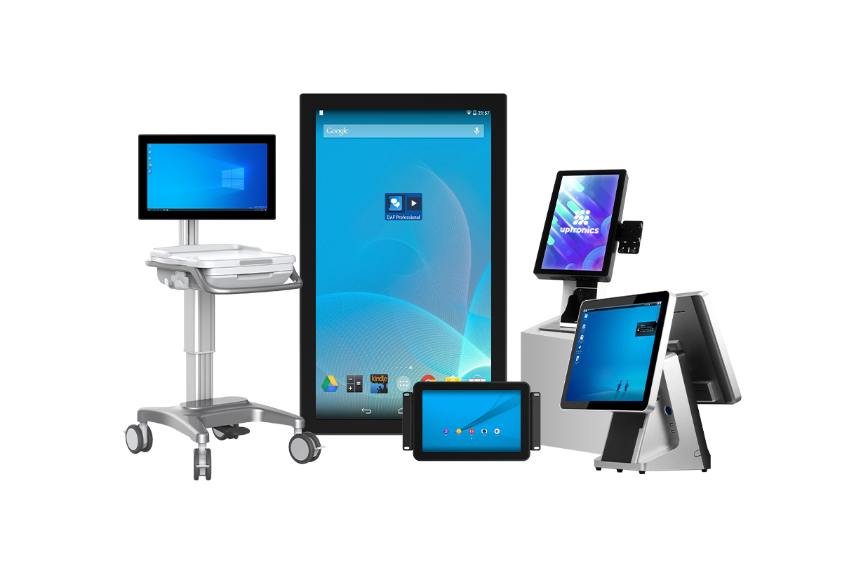
Touch Screen Monitor,Multi Touch Display Monitor,Outdoor Touch Screen Monitor,Waterproof Touch Monitor,Commercial Touch Screen Monitor,KTV Touch Screen Monitor
HuiZhou GreenTouch Technology Co.,Ltd , https://www.bbstouch.com