When using discrete JFETs, the designer may need to adapt a large number of variable device parameters to a given transistor model. The square law equation is generally used as an approximate model of the JFET drain current characteristic: ID = β(VGS-VP)2, where ID is the drain current, VGS is the gate-source voltage, and β is the transconductance parameter, while VP Is the off voltage of the gate. Similarly, the zero-drift drain voltage when the gate-source voltage is 0V is obtained by the following equation: IDSS=βVP2, where IDSS is the zero-drift drain current.
Figure 1 is a characteristic diagram of an N-channel JFET showing the possible differences between a group of devices. For example, the 2N4416A datasheet lists cutoff voltages of -2.5V to -6V and zero drift drain currents from 5mA to 15mA. Some device samples can be observed and correlations can be found between these two parameters. The extra curves in the figure show these extremes, while the middle curve may represent a typical case of a -4V cutoff voltage and 8mA zero drift drain current.
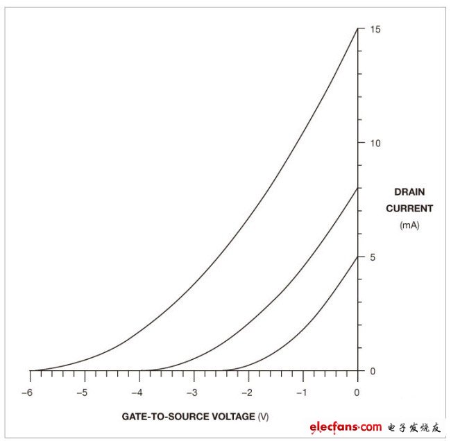
Figure 1. The I series inductance of different N-channel JFET devices may require a significant difference in the 62 D-VGS characteristics.
For mass production circuits, although they can be designed within certain device variations, sometimes a tool is needed to quickly determine the characteristics of a component. This tool can pick a device that is best suited for a circuit, or find a pair of devices that match the parameters quite well.
Figure 2 is a simple test circuit for this purpose. Although the JFET shown in the figure is an N-channel device, the JFET DUT (device under test) can have two polarities through the selection of switch S1. The external voltmeter is connected to the terminal on the right. Switch S2 selects two measurement modes, one is to measure the cutoff voltage and the other is to measure the zero drift drain current. In the cutoff voltage mode, the external meter directly reads the cutoff voltage value; in the zero drift drain current mode, the measured voltage is a zero drift drain current above a 100Ω apparent resistor.
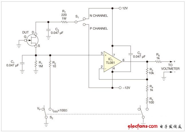
Figure 2, between the DUT source resistors R1 and R2, can be used to measure the cutoff voltage and zero drift drain current.
When S2 is in the cutoff voltage mode, R1 causes a few microamps of drain current to flow into the JFET device under test, and the source voltage is a high approximation of the negative off voltage value. The op amp acts as a unity-gain buffer and performs negative feedback through R3, so an external power meter can be used to directly read the negative cutoff voltage.
In the zero-drift drain current mode, the JFET source-to-ground resistance is only 10Ω, so the drain current is a high approximation of the zero-wrap drain current. The feedback from the op amp is also converted to a configuration with a gain of 10. The feedback divider contains R4 and R5. This gain allows the voltmeter to easily read the small voltage on R2. The reading is the zero drift drain current multiplied by 100Ω. . For example, if the voltmeter reads 1 V, this voltage is equivalent to a 10 mA zero drift drain current.
For an N-channel device, both readings are positive; for a P-channel device, the circuit functions the same, except that the voltage reading is negative. If the JFET to be tested is connected to the circuit with test leads and clips, both of which have some parasitic series inductance, it may be necessary to add a C1 to suppress any tendency to generate high frequency oscillations. R6 isolates the op amp feedback loop from any parasitic capacitance of the voltmeter and its leads, ensuring loop stability. R7 is used to prevent accidental short circuits. A 1.1kΩ resistor can be used instead of R4 and R5. However, you may prefer to use the resistor at hand as shown in the figure.
Taking a sample from a set of JFETs, it is possible to quickly find two parameters by switching the switch and determine which of the JFET parameters falls within the interval shown in Figure 1 to select the device for optimal circuit performance. .

Noah Led Grow Light,Powerful Noah Led Grow Light,Dimmable Noah Led Grow Light,1200W Noah Led Grow Light
Shenzhen Mingxue Optoelectronics CO.,Ltd , https://www.led-lamp-china.com