Clearly compare the structure of AD, stm32 has 3 AD, each AD has many channels, which channel is configured to which channel, here is the timer, there are many timers TIMx, each timer has many CHx (channel ), can be configured as input capture ------- measurement frequency, can also be configured as output comparison -------- output PWM use
Input Capture: Can be used to capture external events and give them time stamps to indicate when this event occurred.
The trigger signal generated by the external event is input by the corresponding pin in the MCU (specifically, it can refer to the datasheet of the MCU), or it can be realized by the analog comparator unit.
Time stamps can be used to calculate frequency, duty cycle, and other characteristics of the signal, as well as to create a log for the event, primarily to measure the frequency of the external signal.
Output comparison: The timer count register is automatically counted after initialization. Count from bottom to top. And there are different working modes.
There is also a compare register. Once the count register matches the compare register during the count from bottom to top, a compare interrupt is generated (when the compare interrupt is enabled).
The count register will then be cleared or counted to the top value depending on the operating mode.
1. Friends, can you explain the working principle of input capture?Quite simply, when the capture you set starts, the CPU will copy the value of the count register to the capture compare register and start counting. When the level change is captured again, this is the value in the count register minus the copy just copied. The value is the duration of this level, and you can set either a rising edge capture, a falling edge capture, or a rising edge falling edge capture. It is not very useful, the most commonly used to measure frequency.
Is the initial value of the count register written in by yourself?
Yes, but don't write by default
If I capture the rising edge, the two values ​​are subtracted, representing the time of the two rising edges in the middle of the level. Right?
Yes
TImer1 has five channels (corresponding to five IO pins), and at the same time, only one pin value can be captured, right?
That's for sure, the channel is much like the ADC channel and can be switched.
The principle of output comparison can you help me introduce it?
There are two units here: a counter unit and a comparison unit. The comparison unit is a double buffer register. The value of the comparison unit can be set according to different modes. At the same time, the counter is constantly counting and does not stop. Compare with the value in the compare register. When the value of the counter is equal to the value of the compare register, a compare match occurs. According to the setting of the counter, if the match is io, the io level is inverted, low, or high. Generate different waveforms.
Is the value of the comparison unit artificially set?Yes, but he will initialize your compare match register based on the configuration of your control registers.
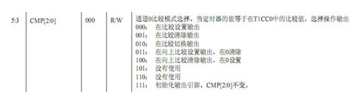
The above does not always understand, it seems that there are not only the few situations you said: "If the match is io level inversion, lower, or higher, it will produce different waveforms."
Is it better to match the IO level you want? Is it cleared or set? Still how? In this way, the waveform can be generated. Otherwise, what is the use of the comparison unit?
Set the output to be set to 1, clear the output is set to 0, switch the output is to reverse the original level, right?
Yes, you understand very quickly
011: Set the pin to 1 when the counter reaches the maximum value. When it reaches 0, the pin level is set to 0, right?
Yep
How to use the output compare mode of Timer 1. Use this function to output a 1KHZ, how to write a program with a duty cycle of 10%? Ask for advice
1, the function of accompanying timer 1 is a special function, not ordinary IO in PERCFG here
2, P1SEL pin selection
3, P1DIR is set to output
4, T3CC0 set cycle
5, T3CC1 set duty cycle
6, T3CCTL0 set channel 0
7, T3CCTL1 set channel 1
8, T3CTL is set to mode
9, open with T3CTL
************ The following is an application that uses a timer as a frequency source to measure the frequency with a timer! ! ! ***********
Debugging the STM32 timer for several days, it is also a clear understanding of the STM32 timer. I need to measure the frequency of the 4 signals and then transfer the frequency of the signal to the memory area via DMA. The manual says that each timer has 4 independent channels. Then I wondered if I could connect these 4 signals to the 4 channels of a timer. In theory, it should be the line of communication. At the beginning, I used the 123 channel of the TIM2 and the 2 channels of the TIM4 to measure the frequency. Since there is no frequency generator, I use tim3 as the signal source. It is OK to use TIM2 and TIM4 to measure (just 4 channels).
Please see the beginning of the program, taking the 1,3 channel of TIM2 as an example (the same as the 2-channel setting method):
TIM_ICInitStructure.TIM_ICMode =TIM_ICMode_ICAP; //Configure as input capture mode
TIM_ICInitStructure.TIM_Channel =TIM_Channel_1; //Select channel 1
TIM_ICInitStructure.TIM_ICPolarity =TIM_ICPolarity_Rising; //Input rising edge capture
TIM_ICInitStructure.TIM_ICSelection =TIM_ICSelection_DirectTI; //Channel direction selection
TIM_ICInitStructure.TIM_ICPrescaler =TIM_ICPSC_DIV1; //A capture is triggered each time a capture input is detected
TIM_ICInitStructure.TIM_ICFilter =0x0; //Filter
TIM_ICInit(TIM2, &TIM_ICInitStructure); //TIM2 channel 1 is configured
TIM_ICInitStructure.TIM_ICMode = TIM_ICMode_ICAP; //Configured as input capture mode
TIM_ICInitStructure.TIM_Channel =TIM_Channel_3; //Select channel 3
TIM_ICInitStructure.TIM_ICPolarity =TIM_ICPolarity_Rising; //Input rising edge capture
TIM_ICInitStructure.TIM_ICSelection =TIM_ICSelection_DirectTI; //
TIM_ICInitStructure.TIM_ICPrescaler =TIM_ICPSC_DIV1; //A capture is triggered each time a capture input is detected
TIM_ICInitStructure.TIM_ICFilter = 0x0; //Filter
TIM_ICInit(TIM2, &TIM_ICInitStructure); //TIM2 channel 3 is configured
Above is the input capture configuration
The work that still needs to be done is (refer to the block diagram of the TIM in the stm32 reference manual):
TIM_SelectInputTrigger(TIM2, TIM_TS_TI1FP1); //Refer to the TIM structure diagram to select the filtered TI1 input as the trigger source, triggering the reset of the following program
TIM_SelectSlaveMode(TIM2,TIM_SlaveMode_Reset); //Reset mode - The rising edge of the selected trigger input (TRGI) initializes the counter and generates an update line number
TIM_SelectMasterSlaveMode(TIM2,TIM_MasterSlaveMode_Enable);
/ / Master-slave mode selectionSo we can easily get the frequency of the signal connected to channel 1 of TIM2, but the value of the frequency of 3 channels is always inaccurate, and the root cause has not been found for a long time. Please see TIM Part of the block diagram
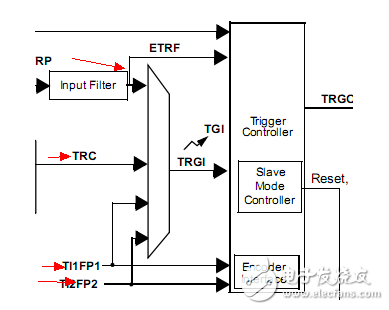
The red arrow indicates that this is the reason. The trigger source only has these four types. The value of the counter on channel 3 cannot be reset when the rising edge of the signal is received. The reason is found. This is the reason why the data on the 3 channels is beating. If there is a way to get the frequency of the signal, you can take the difference between the values ​​captured twice. This value is the period of the signal. You can calculate the frequency according to the actual situation.
There are above to get:
The four channels of stm32's TIM2 can be configured as input capture mode at the same time, but the frequency of CH3 and CH4 signals is a bit cumbersome (take the difference between before and after capture), but his CH1, and CH2 can be easily obtained:
Channel 1
TIM_SelectInputTrigger(TIM2, TIM_TS_TI1FP1); //Refer to the TIM structure diagram to select the filtered TI1 input as the trigger source, triggering the reset of the following program
TIM_SelectSlaveMode(TIM2,TIM_SlaveMode_Reset); //Reset mode - The rising edge of the selected trigger input (TRGI) initializes the counter and generates an update line number
The value of TIMx-"CRR1 is the period of the signal
Channel 2:
TIM_SelectInputTrigger(TIM2, TIM_TS_TI2FP2); //Refer to the TIM structure diagram to select the filtered TI1 input as the trigger source, triggering the reset of the following program
TIM_SelectSlaveMode(TIM2,TIM_SlaveMode_Reset); //Reset mode - The rising edge of the selected trigger input (TRGI) initializes the counter and generates an update line number
The value of TIMx-"CRR2 is the period of the signal
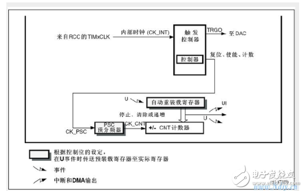
The STM32's timer peripherals are powerful beyond imagination, and the STM32 has a total of eight 16-bit timers. TIM6 and TIM7 are basic timers; TIM2, TIM3, TIM4, and TIM5 are general-purpose timers; TIM1 and TIM8 are advanced timers. These timers make the STM32 with timing, signal frequency measurement, signal PWM measurement, PWM output, three-phase 6-step motor control and encoder interface, all of which are tailor-made for the industrial control field.
Basic timer: With the most basic timing function, the following is its structure:
Let's take a look at its startup code:
Void TIM2_Configuration(void)
{ Structure of the timing configuration of the basic timer TIM2 (including all elements of the timer configuration such as: TIM_Period = count value)
TIM_TimeBaseInitTypeDef TIM_TimeBaseStructure;
Set TIM2_CLK to 72MHZ (that is, the TIM2 peripheral is hung on APB1 and its clock is turned on.)
RCC_APB1PeriphClockCmd(RCC_APB1Periph_TIM2, ENABLE);
Set the count value to 1000
TIM_TimeBaseStructure.TIM_Period=1000;
Divide TIM2_CLK to 72 MHz divided by 72 = 1 MHz for the count frequency of the timer
TIM_TimeBaseStructure.TIM_Prescaler= 71;
This TIM_ClockDivision is to set the clock split, here is not divided or the counting frequency of 1MHZ
TIM_TimeBaseStructure.TIM_ClockDivision=TIM_CKD_DIV1;
Set to count up mode; (count mode has up, down, center aligned 1, center aligned 2, center aligned 3)
TIM_TimeBaseStructure.TIM_CounterMode=TIM_CounterMode_Up;
Put the configured settings into the library file of stm32f10x-tim.c
TIM_TimeBaseInit(TIM2,&TIM_TimeBaseStructure);
Clear flag
TIM_ClearFlag(TIM2, TIM_FLAG_Update);
Enable TIM2 interrupt
TIM_ITConfig(TIM2, TIM_IT_Update, ENABLE);
Enable TIM2 peripherals
TIM_Cmd(TIM2, ENABLE);
}
General purpose timer: It is much more complicated than the basic timer. In addition to the basic timing, it is mainly used to measure the frequency of the input pulse, pulse width and output PWM pulse, and also has an encoder interface.

Let's explain in detail: how to generate PWM pulses
The general-purpose timer can use the GPIO pin for pulse output. When configured as a comparison output and PWM output function, the capture/compare register TIMx_CCR is used as a comparison function. Hereinafter, it is simply referred to as a comparison register.
Here is a direct example of the PWM output operation of the timer: if the configuration pulse counter TIMx_CNT is counted up, and the reload register TIMx_ARR (equivalent to the value N of the TIM_Period of the library function) is configured as N, that is, the current count value of TIMx_CNT X is continuously accumulated under the driving of the TIMxCLK clock source. When the value X of TIMx_CNT is greater than N, the TIMx_CNT value is reset to 0 and recounted.
While the TIMxCNT counts, the count value X of the TIMxCNT is compared with the value A pre-stored by the comparison register TIMx_CCR. When the value X of the pulse counter TIMx_CNT is smaller than the value A of the comparison register TIMx_CCR, the output is high (or low). Flat) Conversely, when the value X of the pulse counter is greater than or equal to the value A of the comparison register, a low level (or a high level) is output.
In this cycle, the obtained output pulse period is the value (N+1) stored in the reload register TIMx_ARR multiplied by the clock period of the trigger pulse, and the pulse width is the value A of the comparison register TIMx_CCR multiplied by the clock period of the trigger pulse, that is, The duty cycle of the output PWM is A/(N+1).
If you don't want to see it, you can directly see the red font I marked, which is generally understandable.
Let's write the specific code and explain:
Void TIM3_GPIO_Config(void)
{Configure TIM3 multiplexed output PWM IO
GPIO_InitTypeDefGPIO_InitStructure;
Turn on the clock of the TIM3
RCC_APB1PeriphClockCmd(RCC_APB1Periph_TIM3, ENABLE);
Turn on the clock of GPIOA and GPIOB
RCC_APB2PeriphClockCmd(RCC_APB2Periph_GPIOA| RCC_APB2Periph_GPIOB, ENABLE);
Configure the working mode of PA6.PA7
GPIO_InitStructure.GPIO_Pin= GPIO_Pin_6 |GPIO_Pin_7;
GPIO_InitStructure.GPIO_Mode = GPIO_Mode_AF_PP;
GPIO_InitStructure.GPIO_Speed ​​= GPIO_Speed_50MHz;
GPIO_Init(GPIOA,&GPIO_InitStructure);
Configure the working mode of PB0.PB1
GPIO_InitStructure.GPIO_Pin= GPIO_Pin_0 |GPIO_Pin_1;
GPIO_Init(GPIOB,&GPIO_InitStructure);
}
Void TIM3_Mode_Config(void)
{
TIM_TimeBaseInitTypeDef TIM_TimeBaseStructure; / / initialize the time base unit of TIM3
TIM_OCInitTypeDef TIM_OCInitStructure; / / initialize the peripherals of TIM3
U16 CCR1_Val= 500;
U16 CCR2_Val= 375;
U16 CCR3_Val= 250;
U16 CCR4_Val= 125; / / PWM signal level jump value (that is, after counting this value is low level before high level)
TIM3 time base unit setting (such as count termination value: 999, starting from 0; counting mode: counting up)
TIM_TimeBaseStructure.TIM_Period= 999;
TIM_TimeBaseStructure.TIM_Prescaler= 0;
TIM_TimeBaseStructure.TIM_ClockDivision= TIM_CKD_DIV1 ;
TIM_TimeBaseStructure.TIM_CounterMode= TIM_CounterMode_Up;
TIM_TimeBaseInit(TIM3,&TIM_TimeBaseStructure);
TIM3 peripheral settings
TIM_OCInitStructure.TIM_OCMode= TIM_OCMode_PWM1; //TIM Pulse Width Modulation Mode 1
TIM_OCInitStructure.TIM_OutputState= TIM_OutputState_Enable;//This is temporarily unknown, not found in the stm32 firmware library. Should be the meaning of the timer output declaration enable
TIM_OCInitStructure.TIM_Pulse =CCR1_Val;//Set the pulse value to be loaded into the capture compare register
TIM_OCInitStructure.TIM_OCPolarity= TIM_OCPolarity_High; //TIM output is relatively high polarity
TIM_OC1Init(TIM3,&TIM_OCInitStructure);
TIM_OC1PreloadConfig(TIM3,TIM_OCPreload_Enable);//Enable or disable TIMx preload register on CCR1
The following three PWM outputs are no longer explained in the same way as above.
TIM_OCInitStructure.TIM_OutputState= TIM_OutputState_Enable;
TIM_OCInitStructure.TIM_Pulse =CCR2_Val;
TIM_OC2Init(TIM3,&TIM_OCInitStructure);
TIM_OC2PreloadConfig(TIM3, TIM_OCPreload_Enable);
TIM_OCInitStructure.TIM_OutputState= TIM_OutputState_Enable;
TIM_OCInitStructure.TIM_Pulse =CCR3_Val;
TIM_OC3Init(TIM3,&TIM_OCInitStructure);
TIM_OC3PreloadConfig(TIM3, TIM_OCPreload_Enable);
TIM_OCInitStructure.TIM_OutputState= TIM_OutputState_Enable;
TIM_OCInitStructure.TIM_Pulse =CCR4_Val;
TIM_OC4Init(TIM3,&TIM_OCInitStructure);
TIM_OC4PreloadConfig(TIM3, TIM_OCPreload_Enable);
TIM_ARRPreloadConfig(TIM3,ENABLE); //Enable TIM3 reload register ARR
TIM_Cmd(TIM3,ENABLE);//Enable TIM3
}
Here is a look at the effect of the 4-way PWM that our program achieves:
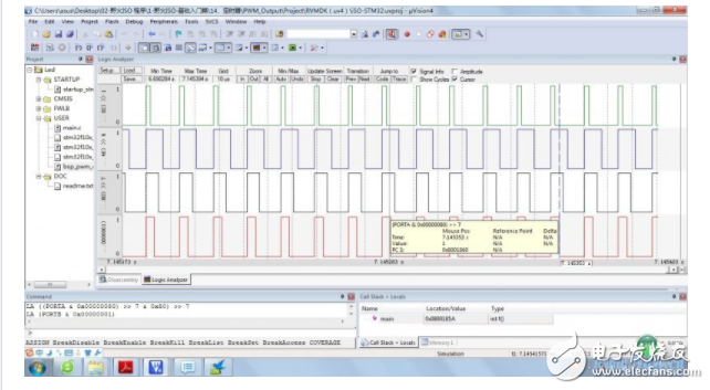
You can see four pwm waves with different duty cycles.
This section is finally finished, personally feel that it is quite easy to understand the code. People who want to see can understand.
Finally add a little pwm specifically what can do? Especially for the majority of electronic DIY enthusiasts:
Motor control for smart cars: we can use pwm to control the speed of our smart cars;
Robot: Give the "robot joint" servo cycle a certain amount (I have forgotten how many milliseconds I have played before) pwm wave can control the steering angle of the servo;
Breathing light: Entering different pwm waves can achieve the effect of lightening and darkening.
There are other applications that everyone can use to add imagination to supplement. We can communicate together and hope that everyone will support you.
The push in terminal the benefit of using this type of terminal block connection is a tool-free connection this allows operators to easily remove and reinsert wire without the need for any type of tool foe the wire that's used on a PIT or push in terminal connection. We to make sure that we're using a ferrule . The ferrule allows for the connection to work properly and seat properly .We simply take the wire with a ferrule connected .We insert it into the push in terminal make sure it is seated fully and there we have a fully and there we have fully seated safe secure connect.
Screw Wire End Terminals,Din Rail Pluggable Terminal Block,DIN Terminal Block,DIN Rail Terminals
Wonke Electric CO.,Ltd. , https://www.wkdq-electric.com