In electronic production and design, inductors with different parameters are often used. The inductance of these coils is not as easy to measure as resistors. Some digital multimeters have inductive measurement, but the measurement range is limited. The circuit measures the inductance value by the resonance method. The lower limit of measurement can reach 10nH, and the measurement range is wide. It can meet the measurement of inductance under normal conditions, the circuit structure is simple, the work is reliable and stable, and it is suitable for enthusiasts.
First, the circuit working principle The circuit principle is shown in Figure 1 (a).
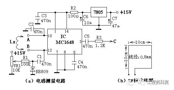
Figure 1 Simple inductance measuring device circuit diagram
The core device of the circuit is the integrated voltage-controlled oscillator chip MC1648, which uses its voltage-controlled characteristic to generate a frequency signal at the output 3 pin, which can indirectly measure the LX value of the inductor to be tested, and the measurement accuracy is extremely high.
BB809 is a varactor. In the figure, potentiometer VR1 divides +15V. Adjusting the potentiometer can obtain different voltage output. This voltage can be added to varactor BB809 through R1 to obtain different capacitance. When measuring the measured inductance LX, just connect LX to the two points A and B in the figure, then adjust the potentiometer VR1 to make the circuit resonate. In the MC1648, the 3rd pin will output the oscillation signal of a certain frequency, and the frequency meter will measure the C point. The frequency value can be calculated by calculating the LX value.
Circuit resonance frequency: f0 = 1/2p
So LX = 1/4p2 f02C
In the formula, the resonant frequency f0 is the output frequency of the 3 pin of the MC1648, and C is the capacitance value of the varactor diode set by the potentiometer VR1. It can be seen that the value of LX needs to know the value of C first. To do this, it is necessary to calibrate the corresponding value of the potentiometer VR1 scale and the varactor.
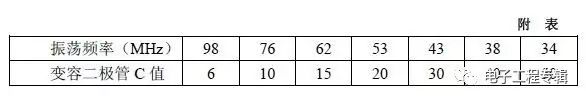
In order to calibrate the capacitance between the varactor and the potentiometer, we have to make a standard square RF (radio frequency) inductor L0. As shown in Figure 6-7(b), the standard coil inductance is 0.44mH. During calibration, connect the RF coil L0 to both ends of A and B of Figure (a), adjust the potentiometer VR1 to different scale positions, measure the corresponding measured value at point C, and calculate the change according to the above resonance formula. The capacitance of the diode on different scales of the potentiometer VR1 dial. The attached table gives the corresponding relationship between the measured samples.
Second, the component selection
The integrated circuit IC can be selected from Motorola's VCO (Voltage Controlled Oscillator) chip. VR1 selects multi-turn high-precision potentiometers. Other components can be selected as shown in the circuit diagram.
Third, the production and debugging method production, you need to make a dial on the multi-turn potentiometer shaft, and bring the pointer. The RF standard coil is self-made according to the dimensions given in Figure (b). The circuit can be installed normally, and the potentiometer VR1 can adjust the corresponding relationship between multiple points of sliding and varactor diodes to ensure convenient measurement. This measurement method is an indirect measurement, but the measurement range is wide and the measurement is accurate, so it is desirable for electronic enthusiasts and laboratories to detect inductance. The device can be turned into a signal generator with an adjustable frequency if the inductor is fixed. Circuit 2 Three-digit display capacitance test table The majority of electronic enthusiasts have this experience. Although the medium and high-end digital multimeter has a capacitance test gear, the measurement range is generally only 1pF~20ïF, which often cannot meet the needs of users. , causing inconvenience to capacitance measurement. The three-digit display capacitance test table introduced by this circuit adopts four integrated circuits. The circuit is simple, easy to manufacture, digital display is intuitive, and the precision is high. The measurement range can reach 1nF~104ïF. Especially suitable for lovers and electrical maintenance personnel to make and use.
First, the circuit working principle The circuit principle is shown as in Fig. 2.
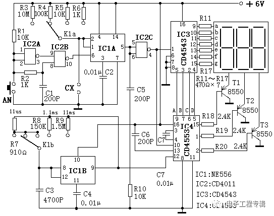
Figure 2 Three-digit display capacitance test chart circuit diagram
The capacitance meter circuit is composed of a reference pulse generator, a capacitance capacity time converter to be tested, a gate controller, a decoder, and a display.
The capacitance capacity time converter to be tested converts the capacity of the measured capacitance into a one-shot time td proportional to its capacity value. The reference pulse generator produces a standard cycle count pulse. The turn-on time of the gate controller is the one-shot time td. During the td time, the cycle count pulse is sent to the back counter through the gate, and the decoder drives the display to display the value. The period T of the counting pulse multiplied by the count value N displayed by the display is the one-shot time td. Since td is proportional to the capacity of the capacitor to be measured, the capacity of the capacitor to be measured is also known.
In Figure 2, the integrated circuit IC1B resistors R7~R9 and capacitor C3 form the reference pulse generator (essentially an unstable multivibrator), and the output pulse signal period T is related to R7~R9 and C3, fixed in C3. In the case of different selections of R7, R8, and R9 by the range switch K1b, three pulse signals having periods of 11 ï, 1.1 ms, and 11 ms can be obtained.
IC1A, IC2, R1~R6, buttons AN and C1 form a time-constant capacitor (substantially a one-shot circuit) to be tested. Pressing AN once, IC10B's 10 pin produces a negative narrow pulse trigger IC1A, and its 5 pin outputs a single high level signal. R3~R6 and the capacitor CX to be tested are single-stability components, and the one-shot time td=1.1 (R3~R6)CX.
IC4, IC2C, C5, C6, R10 form the gate controller and counter. IC4 is CD4553. Its 12-pin is the count pulse input terminal, and the 10-pin is the count enable terminal. CD4553 performs counting at low potential, and 13-pin is count clear. End, the rising edge is valid. When the AN is pressed, the 13 pin of IC4 gets a rising pulse, the counter is cleared, and the 4 pin of IC2C outputs a one-shot low level signal to the 10 pin of IC4, so IC4 counts the reference input from its 12-pin. The pulse is counted. When the one-shot time is over, IC4's 10 pin becomes high level, IC4 stops counting, and finally IC4 passes the counting result of one digit, ten digits, hundred digits by its 9-pin, 7-pin, 6 by time-sharing transmission. The foot and the 5 foot loop output the corresponding BCD code.
IC3 constitutes the decoder driver, which translates the BCD code sent from IC4 into a decimal digital pen segment code, and directly drives the seven-segment digital tube after R11~R17 current limit. The 15th, 1st, and 2nd pins of the integrated circuit CD4553 are digital selection outputs. The pulses are sent to the bases of the transistors T1~T3 through R18~R20 to make them turn on. The two parts are matched to complete the three-digit decimal. Digital Display.
The role of C7 is to generate a rising pulse on R10 when the power is turned on, and the counter is automatically cleared.
Second, in the component selection circuit, IC1 selects NE556; IC2 selects CD4001; IC3 selects CD4543; IC4 selects CD4553. The seven-segment digital tube can be used with a three-word common cathode digital tube. 850 (or other PNP type triode) is used for T1~T3. C1 should not be larger than 0.01ïF, and C3 should use small metallization capacitors. R3~R9 use 1/8W metal film resistor. There are no special requirements for other components, and you can select them according to the circuit labeling.
Third, the production and debugging method After the entire circuit is installed, it can be installed in a plastic box, and the digital tube and the range switch are mounted on the panel. In the production and debugging, the key is to call up the three standard pulse signals of 11ïs, 1.1ms and 11ms. When debugging, you need to adjust the resistance of three resistors, such as R7, R8 and R9, by means of an oscilloscope. These three pulse signals can be conveniently obtained. The resistance values ​​of R7, R8 and R9 in the circuit are experimental data for reference only. The rest of the circuit does not need to be debugged. As long as the good device is selected, the installation is correct, and the corresponding override is marked at the range switch, a practical, accurate and reliable digital capacitance meter can be obtained.
Fourth, the method of use
It should be noted that when using the 1pF~999pF range, the measurement result minus the distributed capacitance value is the accurate value of the measured capacitance due to the influence of the distributed capacitance. The range distribution capacitance value of the capacitance meter can be measured in this way, and the range is set in the range of 1pF to 999pF. When the measured capacitance is not connected, the AN button is pressed, and the measured result is the distributed capacitance value of the block. The value is generally about 10 pF after experimentation. The schedule lists the compositional relationships of the various ranges. Schedule

Circuit 3 Mains voltage bidirectional over-limit alarm protector The alarm protector can perform sound and light alarm when the mains voltage is higher or lower than the specified value, and automatically cut off the electrical power supply to protect the electrical appliance from damage. The device is small in size, full in function, simple in manufacture and practical.
First, the circuit working principle The circuit principle is shown in Figure 3.
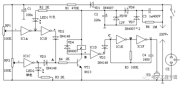
Figure 3 Mains voltage bidirectional over-limit alarm protector circuit diagram Mains voltage one route C3 step-down, DW regulator, VD6, VD7, C2 rectification and filtering output 12V stable DC voltage supply circuit. Another route VD1 rectification, R1 step-down, C1 filtering, generating a voltage of about 10.5V on RP1, RP2 to detect the mains voltage change input signal. The gate IC1A and IC1B form an overvoltage detection circuit, IC1C is undervoltage detection, IC1D is a switch, IC1E, IC1F and piezoelectric ceramic piece YD constitute an audio pulse oscillator. The triode VT and the relay J constitute a protection action circuit. The red LED1 is used as the mains overvoltage indication, and the green tube LED2 is used as the mains undervoltage indication.
When the mains is normal, non-IC1A outputs a high level, IC1B, IC1C output low level, LED1, LED2 are off and no light, VT is off, J does not operate, the appliance is normally powered, B point is high, F4 output Low level, VD5 is on, C is low, the audio pulse oscillator is stopped, and YD is not sounding. When the mains is overvoltage or undervoltage, IC1B and IC1C have one output high level, which makes point A become high potential, VT saturation turns on, J energizes and pulls, disconnects the electrical power supply, and B point becomes Low potential, IC1D output high level, VD5 cut-off, reverse resistance is large, equivalent to open circuit, audio pulse oscillator starts, YD sounds alarm, and the corresponding LED emits light.
Second, the choice of components Integrated chip IC can choose CD74HC04 six inverter, diode VD1 ~ VD6 select IN4007, capacitor C1 ~ C6 select aluminum electrolytic capacitor, withstand voltage 400V, regulator tube selects 12V voltage regulator, relay J selects general 6V DC relay can be used, the resistor uses ordinary 1/8 or 1/4W carbon film resistor, the size can be as shown.
3. When debugging and debugging , use a voltage regulator to supply power, adjust the voltage to normal value (220V), use an incandescent lamp as load, make LED1 and LED2 go out, incandescent light, then adjust the regulator to Limit value or lower limit value, adjust RP1 or RP2 to make LED1 or LED2 just light, and the incandescent light is off, that is, the debugging is successful. All components can be installed in a small plastic box, two holes are fixed on the lid to fix the LED, a larger round hole is used to fix the piezoelectric ceramic piece, and a suitable cap is used to help the piezoelectric piece. The sound chamber makes it sound louder. Circuit 4 Infrared detection burglar alarm This alarm can detect the infrared rays emitted by the human body. When a person enters the monitoring area of ​​the alarm, it can sound an alarm. It is suitable for burglar alarms in important places such as home, office, warehouse, and laboratory.
First, the circuit working principle The circuit principle is shown in Figure 4. The device is composed of an infrared sensor, a signal amplifying circuit, a voltage comparator, a delay circuit and an audible alarm circuit. When the infrared detecting sensor IC1 detects the infrared signal radiated from the front human body, the weak electric signal is output from the 2 pin of the IC1, and is amplified by the first-stage amplifying circuit through the triode VT1, and then input to the operational amplifier IC2 through C2 for high gain. Low noise amplification, at this time the signal output by the IC21 pin is strong enough. IC3 is used as the voltage comparator. Its 5th pin provides the reference voltage from R10 and VD1. When the signal voltage output from IC21 pin reaches the 6th pin of IC3, the voltages of the two input terminals are compared. At this time, the 7th pin of IC3 is from the original The high level goes low. IC4 is the alarm delay circuit, and R14 and C6 form a delay circuit, which takes about 1 minute. When IC3's 7 pin goes low, C6 discharges through VD2. At this time, IC4's pin 2 goes low. It compares with IC4's 3-pin reference voltage. When it is lower than its reference voltage, IC4's The 1 pin becomes high level, VT2 turns on, and the alarm BL energizes to sound an alarm. After the infrared signal of the human body disappears,
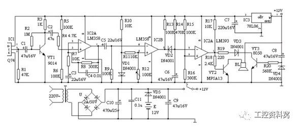
Figure 4 Infrared detection burglar alarm circuit diagram IC3's 7 feet return to high level output, VD2 is cut off at this time. Since the voltage across C6 cannot be abrupt, it is slowly charged to C6 through R14. When the voltage across C6 is higher than its reference voltage, the 1 pin of IC4 becomes low level for about 1 minute, that is, the alarm is continued for 1 minute. . The power-on delay circuit consists of VT3, R20 and C8, and the time is also about 1 minute. Its setting is mainly to prevent the user from immediately alarming after starting the machine, so that the user has enough time to leave the monitoring site and prevent the power failure after the power failure. A false positive occurred while calling. The device is powered by 9-12V DC power supply, step-down by T, full-bridge U rectification, C10 filtering, detection circuit is powered by IC5 78L06, AC and DC, automatic and uninterrupted conversion.
Second, the component selection IC1 uses imported device Q74, the wavelength is 9-10um. IC2 uses the op amp LM358 with high gain and low power consumption. IC3 and IC4 are dual voltage comparators LM393, low power consumption and low offset voltage. In C2 and C5, it is necessary to use a tantalum capacitor with a small leakage electrode, otherwise the debugging will be affected. R12 is a key component for adjusting sensitivity, and a linear high-precision sealing type should be used. Other components can be selected as shown in the circuit diagram.
Third, the production and debugging methods are made, the Fresnel lens is installed in front of the end of the IC1 sensor, because the human body's active frequency range is 0.1-10Hz, the Fresnel lens needs to double the human activity frequency. Installation is correct, connect the power supply for debugging, let a person walk around 7-10m in front of the detector, adjust R12 in the circuit, so that the alarm can be alarmed. As long as the components are of good quality and the welding is correct, the other parts can work normally without debugging. The static working current of the machine is about 10 mA. After the power is turned on for about 1 minute, it enters the waiting state. As soon as someone enters the monitoring area, it will alarm, and the person will stop the alarm about 1 minute after leaving. If the sounder is changed to a relay to drive other devices, it is used for other control. Circuit 5 Non-Smoking Alerts The smoking ban warnings described in this example can be used in homes or in places where smoking is not appropriate (eg hospitals, conference rooms, etc.). When someone smokes, the no-smoking warning device will issue a "Please do not smoke!" language warning to remind the smoker to consciously stop smoking.
First, the circuit working principle The circuit principle is shown as in Fig. 5. The smoke-free warning circuit is composed of a smoke detector, a monostable trigger, a language generator and a power amplifying circuit, and the smoke detector is composed of a potentiometer RP1, a resistor R1 and a gas sensor. The monoflop is composed of a time base integrated circuit IC1, a resistor R2, a capacitor C1, and a potentiometer RP2. The speech generator circuit is composed of a voice integrated circuit IC2, a resistor R3-R5, a capacitor C2, and a Zener diode VS. The audio power amplifying circuit is composed of a transistor V, a boosting power amplifier module IC3, resistors R6 and R7, capacitors C3 and C4, and a speaker BL.
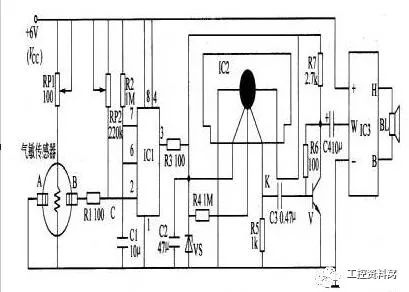
Fig. 5 Circuit diagram of the non-smoking warning device When the smoke sensor detects smoke at the end, the resistance of the two ends of A and B is large, the 2 pin of IC1 is high level (higher than 2Vcc/3), and the output of 3 pin is low. Ping, the voice generator circuit and the audio power amplifier circuit do not work, and the BL does not sound.
When someone smokes and the gas sensor detects smoke, the resistance values ​​of the two ends of A and B become smaller, so that the voltage of pin 2 of IC1 drops. When the voltage of the foot drops to VCC/3, the one-shot trigger Flip, IC1's 3 pin changes from low level to high level. After high level R3 current limit, C2 filtering and VS voltage regulation, 4, 2V DC voltage is generated, which is supplied to voice integrated circuit IC2 and crystal arm. After IC2 is powered on, it outputs a voice electric signal. After the electric signal is amplified by V and IC3, it pushes the BL to issue a "Please do not smoke!" voice warning sound.
Second, the component selection Rl-R7 selects 1/4W carbon membrane resistor or metal membrane resistor. Small linear potentiometers or variable resistors are available for RP1 and RP2. C1, C2 and C4 are all selected from aluminum electrolytic capacitors with a withstand voltage of l6V; C3 is a monolithic capacitor. VS selects 1/2W, 4·2V silicon Zener diode. V selects S9013 or C8050 type silicon NPN transistor for use. IC1 selects NE555 type time base integrated circuit; IC2 selects voice integrated circuit with "Please do not smoke!" voice information; lC3 selects WVH68 type boost power amplifier thick mode integrated circuit. BL uses 8Ω, 1-3W electric speakers. The gas sensor is a MQK-2 type sensor.
Third, the production and commissioning of the anti-smoking warning device, can be used as a smoke alarm to detect fire or as a detection of harmful gases, flammable gases. Adjusting the resistance of RP1 can change the heating current of the gas sensor (generally about 13OmA). Adjusting the resistance of RP2 can change the sensitivity of the monostable trigger circuit action. 6 circuit 555 uses a simple temperature controller circuit according to the circuit substrate is to use an automatic temperature controller 555 IC and a few external components thereof. Because the voltages at various points in the circuit are from the same DC power supply, there is no need for a regulated power supply with good performance, and the capacitor step-down method can work reliably. Circuit components are low in price, small in size, and easy to make in amateur conditions. The temperature automatic controller made by this circuit can be used for industrial heating and electric heating control of households with good effect.
First, the circuit working principle The circuit principle is shown in Figure 6.
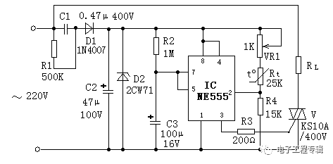
Figure 6. Simple temperature controller circuit diagram with 555 time base circuit. When the temperature is low, the negative temperature coefficient thermistor Rt has a large resistance value. The 555 time base integrated circuit (IC) has 2 pin potentials lower than the Ec voltage. /3 (about 4V), the IC 3 pin outputs a high level, triggers the bidirectional thyristor V to conduct, and turns on the electric heater RL for heating, thereby starting the timing cycle. When the temperature of the thermistor Rt placed at the temperature measuring point is higher than the set value and the timing cycle has not been completed, the heater RL is cut off after the end of the timing period. When the thermistor Rt temperature drops below the set value, the triac V is turned on again, and the electric heater RL is turned on for heating. This will achieve the purpose of automatic temperature control.
Second, the component selection circuit, the thermistor Rt can use the negative temperature coefficient of the MF12 type or MF53 type, you can also choose different resistance values ​​and other models of negative temperature coefficient thermistor, as long as the temperature conditions required The relationship of Rt+VR1=2R4() can be satisfied. The larger the potentiometer VR1 can achieve a larger adjustment range, but the sensitivity will decrease. The triac V can also be selected according to the magnitude of the load current. There are no special requirements for other components, and parameters are selected according to the circuit diagram.
Third, the production and debugging methods The entire circuit can be installed on a circuit board, generally do not need to debug, the time interval is 1.1R2 × C3, should be selected smaller than the heating system's thermal time constant, but it can not be too small, otherwise it will Excessive RF interference is caused by the rapid turn-on or turn-off of the triac V. After installation and commissioning, it can be loaded into a small plastic box and the thermistor Rt can be taken out to the temperature measurement point. Circuit 7 uses an automatic temperature controller of the 555 time base circuit. This circuit can control the state of operation of the powered device by the change of temperature.
First, the circuit working principle The circuit principle is shown in Figure 7.
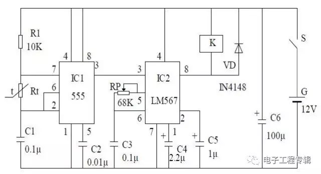
Figure 7: Automatic temperature controller circuit diagram using 555 time base circuit IC1 555 integrated circuit is connected to self-excited multivibrator, Rt is thermistor, when the ambient temperature changes, by resistor R1, thermistor Rt, The oscillation frequency composed of the capacitor C1 will change. The frequency change is sent to the 3 pin of the frequency decoding integrated circuit IC2 LM567 through the 3 pin of the integrated circuit IC1 555. When the input frequency falls exactly at the center frequency of the IC2 integrated circuit, 8 feet Output a low level, so that the relay K is turned on, the contacts are attracted, thereby controlling the on and off of the device to form a temperature control circuit.
Second, the choice of components IC1 selects NE555, μA555, SL555 and other time base integrated circuits; IC2 selects LM567 frequency decoding integrated circuit; VD selects IN4148 silicon switch diode; R1 selects RTX-1/4W type carbon film resistor. C1, C2, C3 select CT1 ceramic capacitor; C4, C5 select CD11-25V type electrolytic capacitor; K selects JZC-22F small medium power electromagnetic relay with working voltage 9V; Rt can use 51KΩ negative temperature coefficient thermal at normal temperature Resistor; RP can be WSW type organic solid fine-tuning variable resistor.
Third, the production and debugging methods In the production process, as long as the circuit is correct, this circuit is very easy to implement, if the component performance is good, you do not need to debug after installation. The circuit 8 adopts the CD4011 over-temperature monitoring automatic control circuit. The circuit has a simple structure and is easy to manufacture. A NAND gate and a thermistor constitute a measurement and control circuit and a siren sound circuit, and a relay is used as an execution circuit.
First, the circuit working principle The circuit principle is shown in Figure 8.

Figure 8 Using the CD4011 over-temperature monitoring automatic control circuit diagram Temperature measuring resistor RT is connected to the input terminal of the control gate D1, it and the resistors R1, R2 and RP through the RP partial pressure adjustment, so that the input level of the gate D1 is high , make D1 output low.
When in use, the thermistor RT is placed on the controlled device. When the temperature of the controlled device exceeds the maximum set temperature, the voltage of the D1 input becomes low due to the small voltage of the RT. After D1 is inverted to a high level, the high level is applied to the control terminal 8 of the multivibrator on the one hand, so that the multivibrator starts to oscillate, and after being amplified by the amplification tube, the siren sound is emitted by the speaker, and is also added to The base of VT1 is turned on, the relay is sucked, and the working power of the controlled device is disconnected through the normally closed contact of the relay; on the other hand, after the D2 is inverted to the low level, the LED of the LED is formed through the light. , LED lighting instructions.
Second, the choice of components IC1 selects CD4011; VD selects IN4001; VS is regulated voltage regulator 10V; VT1 selects 9013, VT2 selects V40AT; capacitor C is 2000P ceramic chip capacitor; relay is 4099 relay; RP selects 470K Ordinary adjustable potentiometer; resistors use 1/8 or 1/4W metal film resistors, BL selects 8Ω, 0.5W electric speakers.
Third, the production and debugging method The temperature measuring resistor RT is placed at the highest limit temperature, adjust the RP, so that the monitoring circuit emits a siren and the relay sucks and works, then the RT is cooled, the siren should stop. Otherwise, the RP should be adjusted repeatedly until it meets the requirements. Circuit 9 Digital Thermometer Circuit This circuit is a thermometer made by applying the integrated temperature sensor of AD590. It has the characteristics of simple structure, reliable use and high precision.
First, the circuit working principle The circuit principle is shown in Figure 9.
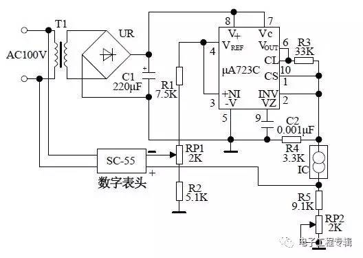
Figure 9 Digital thermometer circuit diagram 100V AC voltage through the transformer T1, rectifier bridge stack UR and capacitor C1, to obtain a DC voltage, and then through the adjustable regulator circuit μA723C to provide a stable operating voltage for the temperature sensor AD590. The AD590 temperature sensor is a new type of current output type temperature sensor consisting of multiple transistors and resistors with the same parameters. When a specific DC operating voltage is applied to both ends of the sensor, if the temperature of the temperature sensor is 1 degree Celsius, the output current of the sensor changes by 1 μA. The changing current of the sensor is converted into a voltage signal through the resistor R5 and the variable resistor RP2, and output to the digital meter, and the temperature change is displayed by a digital meter.
Second, the component selection integrated circuit IC selects the AD590 type temperature sensor. There are no special requirements for other components of this circuit, and can be selected according to the parameters given in the circuit diagram.
Third, the production and debugging methods can change the sensitivity of the output by changing the value of the resistor R5 and the variable resistor RP2. Circuit 10 Tropical fish tank water temperature automatic controller Tropical fish tank water temperature automatic controller uses a negative temperature coefficient thermistor as a temperature probe to automatically heat the fish tank through heating gas. The transient time of this circuit is small, which is beneficial to temperature control accuracy and is applicable to fish tanks of various sizes.
First, the circuit works The circuit diagram shown in Figure 10. After the diodes VD2~VD5 are rectified and the capacitor C2 is filtered, a voltage of about 12V is supplied to the control portion of the circuit. The 555 time base circuit is connected to a monostable flip-flop with a transient state of 11 s. Set the control temperature to 25oC, by adjusting the potentiometer RP so that RP + Rt = 2R1, Rt is a thermistor with a negative temperature coefficient. When the temperature is lower than 25oC, the resistance of Rt rises, and the 2 pin of the 555 time base circuit is low level, then the 3 pin changes from the low level output to the high level output, the relay K is turned on, and the contacts are attracted. The heating tube starts to heat until the temperature returns to 25oC, the resistance of Rt becomes smaller, the 2 pin of the 555 time base circuit is at a high level, the 3 pin outputs a low level, the relay K loses power, the contact is disconnected, and the heating stops.
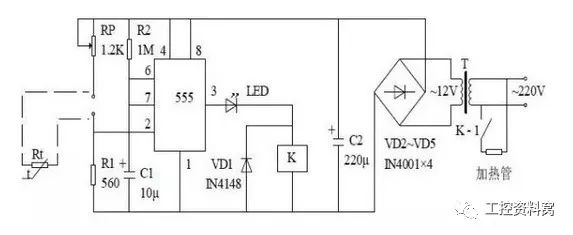
Figure 1 0 Tropical fish tank water temperature automatic controller circuit diagram 2, component selection IC selects NE555, μA555, SL555 and other time base integrated circuits; VD1 selects IN4148 silicon switch diode; LED selects ordinary light-emitting diode; VD2~VD5 selects IN4001 type silicon rectifier Diode; Rt selects 470Ω MF51 type negative temperature coefficient thermistor at room temperature; RP selects WSW organic solid trimmer potentiometer for RW; RXT-1/8W type carbon film resistor for R1 and R2; CD11-16V type for C1 and C3 Electrolytic capacitor; C2 selects CT1 ceramic capacitor; K selects JZC-22F small medium power electromagnetic relay with working voltage 12V.
Third, the production and debugging method Temperature sensing probe with a plastic wire to connect the thermistor Rt, and then seal the solder joint with Rt with epoxy glue, so that it is not afraid of water erosion. This circuit is easy to implement as long as the circuit is correct during the manufacturing process. If the component performance is good, it can be used without debugging after installation. The circuit 11 adopts the simple long delay circuit of the 555 time base circuit. Compared with the general timing circuit, this circuit adds a diode VD1 at the 5th pin of the 555 time base circuit to make the timing time prolonged.
First, the circuit working principle The circuit principle is shown in Figure 11.
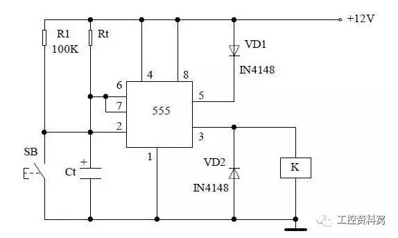
Figure 11 Simple long-delay circuit diagram using 555 time-base circuit When the button SB is pressed, the 12V power supply charges the capacitor Ct through the resistor Rt, so that the potential of the 6-pin is continuously raised, and when the potential of the 6-pin is raised to 5 feet At the potential of the circuit, the circuit reset timing ends. Since a diode VD1 is placed on the 5-pin string to increase the potential of the 5-pin, it has a longer timing than the normal connection (floating or grounding through a small capacitor).
Second, the selection of components 555 circuit selects NE555, μA555, SL555 and other time base integrated circuits; diode VT1, VT2 selects 4148 type silicon switch diode; resistor R1, Rt selects RTX-1/4W type carbon film resistor; capacitor Ct Electrolytic capacitors are selected; relay K can be selected according to the needs of the electrical equipment.
Third, the production and debugging method circuit timing can be adjusted by adjusting the parameter values ​​of the resistor Rt, capacitor Ct to change the length of the timing. The structure of the circuit is simple, as long as the welding according to the circuit diagram, the selected components are correct and can work normally. Circuit 12 Dual 555 Time Base Circuit Long Delay Circuit This circuit forms a timing circuit with a long timing time and adjustable timing by using two 555 time base circuits.
First, the circuit working principle The circuit principle is shown in Figure 12. The IC1 555 time base circuit is connected to a self-excited multivibrator with adjustable duty cycle. When the button SB is pressed, a DC voltage of 12V is applied to the circuit. Since the voltage of the capacitor C6 cannot be abruptly changed, the 2 pin of the IC2 circuit is at a low level, the IC2 circuit is in a set state, and the 3 pin outputs a high level, the relay When K is energized, contacts K-1 and K-2 are closed, K-1 contacts are closed to form a self-locking state, and K-2 contacts are connected to electrical equipment to control the function of turning on and off the electrical equipment.
At the same time, the IC1 555 time base circuit begins to oscillate, so the 3 feet alternately output high and low levels. When the 3-pin output is high, the capacitor C3 is charged through the diode VD3 and the resistor R3. When the 3 pin outputs low level, the diode VD3
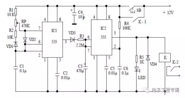
Figure 12 The dual 555 time base circuit long delay circuit diagram is cut off, C3 is not charged, so C3 is charged only when pin 3 is high, so the charging time of capacitor C3 is longer. When the potential of the capacitor C3 rises to 2/3VDD, the IC2 555 time base circuit is reset, the 3 pin output is low level, the relay K is de-energized, the contacts K-1, K-2 are disconnected, and the initial state is restored. Prepare for the second time.
Second, the choice of components IC1, IC2 select NE555, μA555, SL555 and other time-based integrated circuits; VD1 ~ VD4 select IN4148 silicon-type switching diode, LED can use general LED; R1 ~ R5 select RTX - 1/4W type Carbon film resistors; capacitors C1, C2, C5, C6 select CT1 type ceramic capacitors, C4 selects CD11-16V electrolytic capacitors, C3 selects tantalum electrolytic capacitors with extremely small leakage current; RP can use WSW type organic solid fine-tuning variable resistors The relay K selects the JRX-13F type small electromagnetic relay with two sets of switching contacts.
Third, the production and debugging methods In the debugging, you can adjust the variable resistor RP to change the duty cycle of the square wave pulse output of the IC1 555 time base circuit 3, thus changing the timer timing. The structure of the circuit is simple, as long as the welding according to the circuit diagram, the selected components are correct and can work normally. Circuit 13 Accurate long delay circuit This circuit is composed of CD4060 timer base time circuit. The timing time base pulse generated by the circuit is divided by the internal frequency divider to output the time base signal. The frequency division circuit of the peripheral is divided to obtain the required timing control time.
First, the circuit working principle The circuit principle is shown in Figure 13. After power-on, the time-base oscillator oscillates and is frequency-divided to output the time base signal. IC2, which is a frequency divider, starts counting the division. When the count reaches 10, Q4 outputs a high level, and the high level is inverted to a low level by D1 to turn off VT, and the relay is powered off to cut off the operating power of the controlled circuit. At the same time, the D1 output is hungry low and is inverted to the high level by D2 and then applied to the CP terminal of IC2, so that the output high level of the output is maintained. After the circuit is energized to reset IC1 and IC2, the four output terminals of IC2 are low. The low level of the Q4 output is inverted by D1, the VT is turned on through R4, and the relay is energized and summed. This working state is the power-on state and the time-off state.
Second, the component selection IC1 selects CD4060, IC2 selects CD4518, IC3 selects CD4069; VT1 selects 9013, 9014; C1 selects

Figure 13: Accurate long-delay circuit diagram with ceramic chip capacitors, C2 and C3 select aluminum electrolytic capacitors with a withstand voltage of 15V; relays use model JZC-6F DC relays; RP selects 200K ordinary adjustable potentiometers; resistors use 1/8 or 1 /4W metal film resistors, SA1 and SA2 are small toggle openings.
Third, the production and debugging methods If you want to change the power-on disconnection, timing state, you can add a level of inverter between the output D1 and VT. The length of the timing can be adjusted by the RP, or by the connection of the output of the IC2 according to the correspondence of the second-decimal encoding. The timing range of this example circuit is: 3min~1h. Circuit 14 Digital Long Delay Circuits Generally, long delay circuits typically rely on electrolytic capacitors or high impedance circuits. The stability of such delay circuits is poor, and the accuracy of delay is not high. What is presented here is a digital long delay circuit that completely eliminates large electrolytic capacitors and high impedance circuits with high delay accuracy.
First, the circuit working principle The circuit principle is shown in Figure 14.

Figure 14 digital long delay circuit diagram
At the heart of the circuit is the integrated block MCI4521B, which is a 24-stage crossover circuit with an inverter that forms the oscillating circuit. If the trigger input is grounded or no signal is applied, the circuit enters a delay state, which is adjusted by the range switch X and 100KΩ potentiometer.
If X is connected to point A, the delay is 1 minute 40 seconds to 18 minutes 30 seconds, and X is connected to B, and the delay is 13 minutes 20 seconds to 2 hours 28 minutes. When X is connected to point C, the delay is 1 hour 47 minutes to 20 hours. The specific delay time is set by a 100KΩ potentiometer. If a longer delay is required, a large capacitor can be used instead of the 39nF capacitor. At this time, the delay can be more than one week. When a positive signal is applied to the trigger output, the divider in 4521B is reset.
Second, the component selection and production IC selects MCI4521B integrated circuit; Rl~R4 selects 1/4W metal film resistor for use; RP selects organic solid variable resistor. C1 uses ceramic chip capacitors. VD1 selects IN4004 type silicon rectifier diode for use; VD2 selects type IN4148 type silicon switch diode for use. VT selects BC337 type silicon triode; VS selects 1W, 15V silicon steady voltage diode. Connect the circuit as required, and basically work without debugging. The delay is reliable and stable. It is recommended to be powered by a 6~15V regulated power supply. Circuit 15 Cycle Operation Timing Controller This circuit can set the cycle time of the equipment and the time of each operation. It can let the equipment continuously cycle according to the set time. It can be applied to timing pumping, timing ventilation, timing ventilation, etc. Control the occasion.
First, the circuit working principle The circuit principle is shown in Figure 15.
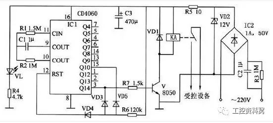
Figure 15 Circuit diagram of the cyclic operation timing controller The circuit is stepped down by the capacitor C2 and the bleeder resistor R3. After the rectifier is rectified by the bridge IC2, the VD2 is regulated to obtain a DC voltage of about 12V to supply power to the IC1 and other circuits. IC1 is a 14-bit binary counter/divider integrated circuit that provides a clock pulse for IC1 timing by a clock oscillator of a certain frequency formed by the internal circuits of R1, R2, C1, and IC1. When the circuit is energized, it first enters the working gap waiting time of the device. IC1 internally realizes the delay by counting and dividing the clock pulse. When the timing time is up (according to the parameter in the figure, it is about 3 hours), the Q14 end of IC1 The output is high, so that the transistor V is turned on, and the relay KA gets a point to drive the controlled device to start working. At this point, IC1 starts to count the working time of the device again. When the timing time is up (about 20 minutes according to the parameters in the figure), the Q14 end of IC1 changes to low level again, so that V is cut off and the device stops working. At this time, IC1 is automatically reset, and the next timing is started again, so that the device can perform the timing cycle according to the set time. In the figure, VL is the work indicator.
Second, the component selection IC IC1 selects the 14-bit binary count/divider integrated circuit CD4066, can also use CC4066 or other digital circuit integrated blocks with the same function. IC2 selects 1A, 50V bridge stack, and can also be connected with four 1N4007 diodes. Transistor V uses NPN type triode 8050, and can also use domestic triodes such as 9013 or 3DG12. VD1 selects rectifier diode 1N4007; VD1 selects 1W, 12V silicon voltage regulator tube, such as 1N4742; VD3 ~ VD5 uses switching diode 1N4148; VL selects ordinary light-emitting diode. Resistors R1, R2, R4, R6 and R7 use 1/4W metal film resistors; R3 and R5 use 1/2W carbon film resistors. C1 selects polyester or monolithic capacitors; C2 selects polypropylene capacitors with a withstand voltage of 450V and above; C3 selects aluminum electrolytic capacitors with a withstand voltage of 16V. KA选用线圈电压为12V的微型继电器,触点容é‡æ ¹æ®å—控设备的功率æ¥ç¡®å®šã€‚
三ã€åˆ¶ä½œä¸Žè°ƒè¯•æ–¹æ³•ç”µè·¯å®‰è£…完æˆåŽï¼Œä¸€èˆ¬æ— 需调试å³èƒ½æ£å¸¸å·¥ä½œã€‚当需è¦è°ƒèŠ‚控制时间时,å¯è°ƒèŠ‚R1ã€å’ŒC1çš„å‚数;也å¯æ”¹å˜IC1输出控制端(Q4~Q14)的ä½ç½®æ¥å®žçŽ°ã€‚ 电路16 多级循环定时控制器该电路是一个三级定时控制器,å¯ç”¨äºŽæŽ§åˆ¶ä¸‰å°è®¾å¤‡æŒ‰ç…§è®¾å®šçš„时间ä¾æ¬¡å¾ªçŽ¯å·¥ä½œï¼Œè€Œä¸”æ¯å°è®¾å¤‡çš„工作时间å¯ä»¥ç‹¬ç«‹è°ƒèŠ‚,如果需è¦æŽ§åˆ¶æ›´å¤šè®¾å¤‡å¾ªçŽ¯å®šæ—¶å·¥ä½œï¼Œåªéœ€è¦å¢žåŠ å•å…ƒç”µè·¯çš„æ•°ç›®å³å¯ã€‚电路工作稳定ã€æ€§èƒ½ä¼˜è‰¯ã€æ€§ä»·æ¯”高ã€æ“作方便ã€é€‚åˆä¸ªäººå’Œå°åž‹ä¼ä¸šåˆ¶ä½œã€‚å¯ç”¨äºŽä¼ä¸šç”Ÿäº§è‡ªåŠ¨æŽ§åˆ¶åŠå½©ç¯æŽ§åˆ¶ï¼Œä¹Ÿå¯ç”¨äºŽå®¶ç”¨ç”µå™¨çš„趣味控制ç‰ã€‚
一ã€ç”µè·¯å·¥ä½œåŽŸç†ç”µè·¯åŽŸç†å¦‚图16所示。
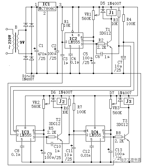
图16 多级循环定时控制器电路图电路ä¸ï¼Œç”±ä¸‰ä¸ªæ—¶åŸºé›†æˆç”µè·¯LM555组æˆä¸‰ä¸ªå•ç¨³æ€ç”µè·¯ï¼Œæ¯ä¸ªå•ç¨³æ€ç”µè·¯ä½œä¸ºä¸€ä¸ªå®šæ—¶æŽ§åˆ¶å•å…ƒã€‚三个å•å…ƒå…±åŒå®Œæˆä¸‰çº§å¾ªçŽ¯å®šæ—¶æŽ§åˆ¶åŠŸèƒ½ã€‚在接通电æºçš„瞬间,由于555集æˆç”µè·¯IC3å’ŒIC4çš„å¤ä½ç«¯4脚都接有时间常数较大的自动å¤ä½ç”µè·¯ï¼ˆåˆ†åˆ«ç”±R4ã€C7å’ŒR7ã€C11组æˆï¼‰ï¼Œä½¿IC3å’ŒIC4å¤ä½ï¼Œå®ƒä»¬çš„输出端3脚就输出低电平,使三æžç®¡T2ã€T3分别截æ¢ï¼Œç»§ç”µå™¨J2ã€J3释放。由于IC2å¤ä½ç«¯4脚直接接在电æºæ£æžï¼Œç”µæºæŽ¥é€šæ—¶ç”µå®¹C3上的电压ä¸èƒ½çªå˜ï¼ŒIC2触å‘端2脚得到触å‘电压,使其进入暂稳æ€ï¼Œå…¶3脚输出高电平,三æžç®¡T1导通,继电器J1å¸åˆï¼ŒJ1触头å¯æŽ§åˆ¶ç”µå™¨é€šç”µå·¥ä½œã€‚åŒæ—¶ç”µæºç»ç”µä½å™¨VR1å‘电容C5充电,当C5上的电压å‡é«˜åˆ°ç”µæºç”µåŽ‹çš„三分之二(4V)时,IC2结æŸæš‚稳,其3脚输出低电平使三æžç®¡T1截æ¢ï¼Œç»§ç”µå™¨J1释放,其触头控制的电器æ–电åœæ¢å·¥ä½œã€‚调节电ä½å™¨VR1和电容C5çš„å‚æ•°å°±å¯æ”¹å˜ç»§ç”µå™¨J1çš„å¸åˆæ—¶é—´ã€‚在IC2输出低电ä½çš„瞬间,由电容C6和电阻R3组æˆçš„微分电路,将在IC3的触å‘端2脚产生负尖脉冲,触å‘IC3进入暂稳æ€ï¼Œå…¶è¾“出端3脚输出高电ä½ï¼Œä½¿ä¸‰æžç®¡T2导通,继电器J2å¸åˆï¼Œå…¶è§¦å¤´æŽ§åˆ¶çš„电器通电工作。调节电ä½å™¨VR2和电容C9çš„å‚æ•°å°±å¯æ”¹æš‚稳æ€æ—¶é—´ã€‚当第二å•å…ƒæš‚稳æ€ç»“æŸæ—¶ï¼Œç”±ç”µå®¹C10和电阻R6组æˆçš„微分电路,将在IC4的触å‘端2脚产生负尖脉冲,触å‘IC4进入暂稳æ€ï¼Œå…¶è¾“出端3脚输出高电ä½ï¼Œä½¿ä¸‰æžç®¡T3导通,继电器J3å¸åˆï¼Œå…¶è§¦å¤´æŽ§åˆ¶çš„电器通电工作。调节电ä½å™¨VR3和电容C13çš„å‚æ•°å°±å¯æ”¹æš‚稳æ€æ—¶é—´ã€‚当第三å•å…ƒæš‚稳æ€ç»“æŸæ—¶ï¼Œç»å¾®åˆ†ç”µè·¯C3ã€R1去触å‘第一å•å…ƒç”µè·¯ï¼Œè¿™æ ·ä¾æ¬¡å¾ªçŽ¯æ¥å®žçŽ°å¾ªçŽ¯å®šæ—¶æŽ§åˆ¶ã€‚
二ã€å…ƒå™¨ä»¶é€‰æ‹©ç”µè·¯ä¸ï¼ŒIC1为三端集æˆç¨³åŽ‹ç”µè·¯ï¼Œé€‰æ‹©MC7806åž‹ï¼› IC2ã€IC3ã€IC4采用LM555时基集æˆç”µè·¯ï¼›ç»§ç”µå™¨J1ã€J2ã€J3è¦æ ¹æ®å…¶æŽ§åˆ¶ç”µå™¨çš„工作电æµæ¥é€‰æ‹©ï¼Œä½†ç»§ç”µå™¨çº¿åœˆé¢å®šç”µåŽ‹åº”为直æµ6V。其他元器件没有特殊è¦æ±‚ï¼ŒæŒ‰ç”µè·¯æ ‡æ³¨é€‰æ‹©å³å¯ã€‚
三ã€åˆ¶ä½œä¸Žè°ƒè¯•æ–¹æ³•æ•´ä¸ªç”µè·¯æ£€æŸ¥æŽ¥çº¿æ— 误,通电就能æ£å¸¸å·¥ä½œï¼Œç”µè·¯ä¸çš„VR1ã€C5ï¼›VR2ã€C9ï¼›VR3ã€C13çš„å‚数分别决定三个å•å…ƒç”µè·¯çš„定时时间,按电路å‚数定时时间约为1.1RC秒。 电路17 抗干扰定时器在è¿ç”¨555时基电路设计而æˆçš„定时器电路ä¸ï¼Œä¸€èˆ¬éƒ½å°†555时基电路连接æˆå•ç¨³æ€è§¦å‘å™¨ï¼Œè¿™æ ·è¿žæŽ¥ä½¿å¾—ç”µè·¯è®¾è®¡ç®€å•ï¼Œåªéœ€è¦å‡ 个电阻器和电容器就能实现触å‘功能,但åŒæ—¶ä¹Ÿå˜åœ¨å¤–部对555时基电路2脚的干扰问题,本电路巧妙的利用了555时基电路4脚的强制å¤ä½çš„功能æ¥å®žçŽ°æŠ—干扰的定时器电路。
一ã€ç”µè·¯å·¥ä½œåŽŸç†ç”µè·¯åŽŸç†å¦‚图17所示。
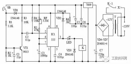
图17 抗干扰定时器电路图在SBæ–开时,555时基电路的4脚通过电阻器R6与地相连,555时基电路被强制å¤ä½ã€‚æ¤æ—¶ï¼Œæ— 论2è„šå—到多大的干扰,555时基电路都ä¸å·¥ä½œã€‚当按下按钮BåŽï¼Œç”µæºé€šè¿‡äºŒæžç®¡VD1åŠ åˆ°4脚一个高电平,时基电路的强制å¤ä½åŠŸèƒ½è§£é™¤ï¼ŒåŒæ—¶ç”µæºé€šè¿‡ç”µé˜»å™¨R1åŠ åˆ°ä¸‰æžç®¡VT1的基æžä¸Šï¼Œä½¿å¾—VT1导通,电容器C2通过与VT1集电æžç›¸è¿žåŽå‘IC电路的2脚输出一个低电平,IC翻转置ä½ï¼Œ3脚输出高电平,å‘光二æžç®¡ç‚¹äº®ã€ç»§ç”µå™¨K得电,触点K-1é—åˆï¼Œæ’座对外供电,åŒæ—¶3脚的高电平通过VD2å‘4脚输出一个高电平使得电路自é”。当暂æ€ç»“æŸåŽï¼Œç”µè·¯ç¿»å›žç¨³æ€ï¼Œ3脚输出低电平,继电器K失电,触头K-1æ–开,电路æ¢å¤åˆ°åˆå§‹çŠ¶æ€ã€‚
二ã€å…ƒå™¨ä»¶çš„选择 IC1 555时基电路选用NE555ã€Î¼A555ã€SL555ç‰æ—¶åŸºé›†æˆç”µè·¯ï¼›R1~R7选用RTX—1/4W型碳膜电阻器;RPå¯ç”¨WSW型有机实心微调å¯å˜ç”µé˜»å™¨ï¼›C2ã€C4ã€C5ã€C6选用CT1型瓷介电容器,C1ã€C3ã€C7选用CD11—16V电解电容器;二æžç®¡VD1ã€VD2ã€VD3选用IN4148硅型开关二æžç®¡ï¼ŒVD4~VD7选用IN4001硅型普通整æµäºŒæžç®¡ï¼›ç»§ç”µå™¨Kå¯æ ¹æ®ç”¨ç”µè®¾å¤‡çš„需è¦é€‰æ‹©ï¼›ä¸‰ç«¯é›†æˆç¨³åŽ‹å™¨é€‰ç”¨7809型三端集æˆç¨³åŽ‹ç”µè·¯ã€‚
三ã€åˆ¶ä½œä¸Žè°ƒè¯•æ–¹æ³•åœ¨ç”µè·¯çš„调试阶段,电路的定时时间å¯ä»¥é€šè¿‡T=1.1(RRP+R5)×C3估算,所以需è¦æ”¹å˜å®šæ—¶æ—¶é—´å¯ä»¥é€šè¿‡è°ƒèŠ‚å¯å˜ç”µé˜»å™¨æ¥å®žçŽ°ã€‚ 电路18 采用555集æˆç”µè·¯çš„简易光电控制器该光电控制器以555时基集æˆç”µè·¯ä¸ºæ ¸å¿ƒï¼ŒæŽ§åˆ¶æ–¹å¼æ¯”较简å•ï¼Œä½¿ç”¨å¯é ã€å¯¿å‘½é•¿ï¼Œæ˜¯ä¸€ç§ä»·æ ¼ä½Žã€ä½“积å°ã€ä¾¿äºŽè‡ªåˆ¶çš„光电控制开关电路。å¯ç”¨äºŽå·¥ä¸šç”Ÿäº§å’Œå®¶ç”¨ç”µå™¨ç‰çš„控制。
一ã€ç”µè·¯å·¥ä½œåŽŸç†ç”µè·¯åŽŸç†å¦‚图18æ‰€ç¤ºã€‚æ— å…‰ç…§å°„æ—¶ï¼Œå…‰æ•ç”µé˜»RG的阻值很大(1MΩ以上),555时基集æˆç”µè·¯çš„2è„šã€6脚电压约为电æºç”µåŽ‹çš„1/2(6V),3脚输出低电平,KAçº¿åœˆæ— ç”µï¼Œç»§ç”µå™¨é‡Šæ”¾ã€‚å½“æœ‰å…‰çº¿ç…§å°„åˆ°å…‰æ•ç”µé˜»RG上时,RG阻值会大幅下é™ï¼ˆå°äºŽ10KΩ),555çš„2è„šã€6

图18 采用555集æˆç”µè·¯çš„简易光电控制器电路图脚电压é™åˆ°ç”µæºç”µåŽ‹çš„1/3(4V)以下,3脚输出高电平,KA线圈得电,继电器å¸åˆï¼Œå³ä½¿å…‰ç…§æ¶ˆå¤±ï¼ŒKAä»ä¿æŒå¸åˆçŠ¶æ€ã€‚
å…¶åŽï¼Œå¦‚å†æœ‰å…‰çº¿ç…§å°„到光æ•ç”µé˜»RG上,则电容C1储å˜çš„电压通过RGåŠ åˆ°555çš„6脚,使6脚的电压大于电æºç”µåŽ‹çš„2/3(8V),3脚输出低电平,KA线圈失电,继电器释放,电路æ¢å¤åˆ°åŽŸå§‹çŠ¶æ€ã€‚å…‰æ•ç”µé˜»RGæ¯å—光照射一次,电路的开关状æ€å°±è½¬æ¢ä¸€æ¬¡ã€‚
二ã€å…ƒå™¨ä»¶é€‰æ‹©åŠåˆ¶ä½œè°ƒè¯• IC用NE555集æˆç”µè·¯ï¼Œ RG应选用亮电阻值≤10KΩ;暗电阻值≥1MΩ的光æ•ç”µé˜»ï¼Œå…¶ä»–å…ƒä»¶æ— ç‰¹æ®Šè¦æ±‚,å„元件å‚æ•°è§ç”µè·¯å›¾ã€‚该电路安装完åŽè£…入一å°å¡‘料盒内,将光æ•ç”µé˜»RG外露,ä¸éœ€è¦è°ƒè¯•å°±å¯æ£å¸¸å·¥ä½œã€‚ 电路19 采用功率开关集æˆç”µè·¯TWH8751çš„è·¯ç¯è‡ªåŠ¨æŽ§åˆ¶å™¨æœ¬ä¾‹ä»‹ç»çš„光控路ç¯ï¼Œåœ¨ç™½å¤©ä¸å·¥ä½œï¼Œå¤œæ™šèƒ½è‡ªåŠ¨ç‚¹äº®ï¼Œå¯ç”¨äºŽè¡—é“或农æ‘场院ç‰åœºåˆã€‚ 一ã€ç”µè·¯å·¥ä½œåŽŸç†ç”µè·¯åŽŸç†å¦‚图19所示。该光控路ç¯ç”µè·¯ç”±ç”µæºç”µè·¯å’Œå…‰æŽ§ç”µè·¯ç»„æˆï¼Œå¦‚图所示。电æºç”µè·¯ç”±ç”µæºå˜åŽ‹å™¨Tã€æ•´æµäºŒæžç®¡VDl-VD4和滤波电容器C组æˆã€‚光控电路由光æ•ç”µé˜»å™¨RGã€ç”µé˜»å™¨R1ã€R2ã€å¯å˜ç”µé˜»å™¨RPã€ç”µå开关集æˆç”µè·¯ICã€ç»§ç”µå™¨K和二æžç®¡VD5组æˆã€‚交æµ220V电压ç»Té™åŽ‹ã€VDl-VD4æ•´æµå’ŒC滤波åŽï¼Œä¸ºå…‰æŽ§ç”µè·¯æä¾›+l2V工作电æºã€‚白天,RGå—光照射而呈低阻状æ€ï¼Œä½¿ICçš„2è„š(选通端)å’Œ4è„š(输出端)å‡ä¸ºé«˜ç”µå¹³ï¼Œå…¶å†…部的电å开关处于截æ¢çŠ¶æ€ï¼ŒKä¸å¸åˆï¼Œè·¯ç¯ELä¸äº®ã€‚夜晚,RCæ— å…‰ç…§å°„å‘ˆé«˜é˜»çŠ¶æ€ï¼ŒICçš„2è„šå˜ä¸ºä½Žç”µå¹³ï¼Œå…¶å†…部的电å开关接通,EL点亮。调节RP的阻值,å¯æ”¹å˜å…‰æŽ§çš„çµæ•åº¦ã€‚
图19 采用功率开关集æˆç”µè·¯TWH8751çš„è·¯ç¯è‡ªåŠ¨æŽ§åˆ¶å™¨ç”µè·¯å›¾äºŒã€å…ƒå™¨ä»¶é€‰æ‹© Rlå’ŒR2选用1/4W金属膜电阻器或碳膜电阻器。RP选用实心å¯å˜ç”µé˜»å™¨ã€‚RG选用RG45系列的光æ•ç”µé˜»å™¨ã€‚C选用è€åŽ‹å€¼ä¸º16Vçš„é“电解电容器。VDl-VD5选用1N400l或lN4007åž‹ç¡…æ•´æµäºŒæžç®¡ã€‚IC选用TWH8751型电å开关集æˆç”µè·¯ã€‚K选用JZX-22Fåž‹(触头电æµè´Ÿè·ä¸ºIOA)l2Vç›´æµç»§ç”µå™¨ï¼Œå¯å°†å…¶ä¸¤ç»„常开触头并è”使用。T选用3-5Wã€äºŒæ¬¡ç”µåŽ‹ä¸ºl2V的电æºå˜åŽ‹å™¨ã€‚
三ã€åˆ¶ä½œä¸Žè°ƒè¯•æ–¹æ³•åˆ¶ä½œæ—¶å¯è‡ªåˆ¶å°åˆ·ç”µè·¯æ¿ï¼Œä¹Ÿå¯ä½¿ç”¨ä¸‡èƒ½å°åˆ·ç”µè·¯æ¿ï¼Œç”µè·¯å®‰è£…完æˆåŽï¼Œåªè¦çº¿è·¯æ£ç¡®ï¼Œä¸€èˆ¬æ— 需调试å³å¯æ£å¸¸ä½¿ç”¨ã€‚ 电路20 采用åŒD触å‘器CD4013çš„è·¯ç¯æŽ§åˆ¶å™¨æœ¬ä¾‹ä»‹ç»çš„光控路ç¯é‡‡ç”¨CD4013åŒD触å‘器集æˆç”µè·¯ï¼Œç”µè·¯ç»“构简å•ã€å®¹æ˜“制作ã€å·¥ä½œç¨³å®šå¯é 。
一ã€ç”µè·¯å·¥ä½œåŽŸç†ç”µè·¯åŽŸç†å¦‚图20所示。
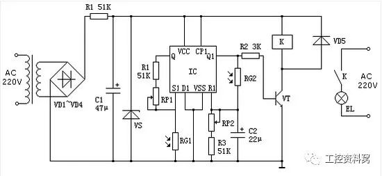
图20 采用åŒD触å‘器CD4013çš„è·¯ç¯æŽ§åˆ¶å™¨ç”µè·¯å›¾è¯¥å…‰æŽ§è·¯ç¯ç”µè·¯ç”±ç”µæºç”µè·¯ã€å…‰æŽ§ç”µè·¯å’ŒæŽ§åˆ¶æ‰§è¡Œç”µè·¯ç»„æˆã€‚交æµ220V电压ç»VD1~VD4æ•´æµã€R1é™æµã€C1滤波åŠVS稳压åŽï¼Œä¸ºå…‰æŽ§ç”µè·¯å’Œæ‰§è¡Œç”µè·¯æä¾›+12V工作电压。
白天,RG1å’ŒRG2å—光照射而呈低阻状æ€ï¼ŒICçš„S1端为低电平,R1端为高电平,1端输出低电平,VT处于截æ¢çŠ¶æ€ï¼ŒK处于释放状æ€ï¼Œç…§æ˜Žç¯ELä¸äº®ã€‚夜晚,RG1å’ŒRG2å› æ— å…‰ç…§å°„æˆ–å…‰ç…§å˜å¼±è€Œé˜»å€¼å¢žå¤§ï¼Œä½¿ICçš„S1端å˜ä¸ºé«˜ç”µå¹³ï¼ŒR1端å˜ä¸ºä½Žç”µå¹³ï¼ŒQ1端输出高电平,VT饱和导通,K通电å¸å’Œï¼Œå…¶å¸¸å¼€è§¦å¤´æŽ¥é€šï¼ŒEL点亮。
天亮åŽï¼ŒRG1å’ŒRG2阻值下é™ï¼ŒICçš„Q1端åˆè¾“出低电平,VT截æ¢ï¼ŒK释放,EL熄ç。
二ã€å…ƒå™¨ä»¶é€‰æ‹© IC选用CD4013或CC4013åž‹åŒD触å‘器集æˆç”µè·¯ï¼ŒVT选用8050或9014åž‹ç¡…NPN晶体管;RG1å’ŒRG2选用MG45系列的光æ•ç”µé˜»å™¨ï¼›VD1~VD5å‡é€‰ç”¨IN4007或IN4004åž‹æ•´æµäºŒæžç®¡ã€‚VS选用1Wã€12V稳压管,C1选用è€åŽ‹25Vçš„é“电解电容,C2选用è€åŽ‹16Vçš„é“电解电容,RP1å’ŒRP2选用普通电ä½å™¨ï¼ŒR1选用2W的金属膜电阻器,R2~R4选用普通1/8或1/4W金属膜电阻器,K选用12Vç›´æµç»§ç”µå™¨ï¼Œå…¶è§¦å¤´ç”µæµå®¹é‡è§†EL功率而定。
三ã€åˆ¶ä½œä¸Žè°ƒè¯•æ–¹æ³•ç”µè·¯å…ƒä»¶é€‰æ‹©æ£ç¡®ï¼Œç„ŠæŽ¥æ— 误åŽï¼Œå³å¯ä½¿ç”¨ï¼Œè°ƒèŠ‚RP1å’ŒRP2的阻值,å¯ä»¥è°ƒèŠ‚光控的çµæ•åº¦ã€‚ 电路21 使用氖ç¯çš„å•é”®è§¦æ‘¸å¼€å…³è§¦æ‘¸å¼ç…§æ˜Žå¼€å…³æ˜¯ä¸€ç§éžå¸¸å®žç”¨çš„电å开关,用手触摸一下导电片,就能实现开关动作,使用方便å¯é ã€ç”µè·¯ç®€å•ã€æ€§èƒ½ç¨³å®šã€å¯¿å‘½é•¿ã€èŠ‚电效果明显。适åˆäºŽçˆ±å¥½è€…自制。
一ã€ç”µè·¯å·¥ä½œåŽŸç†ç”µè·¯åŽŸç†å¦‚图21所示。
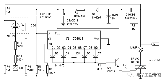
图21 使用氖ç¯çš„å•é”®è§¦æ‘¸å¼€å…³ç”µè·¯å›¾æŽ¥é€šç”µæºåŽï¼Œå› C3ã€R5的微分作用,CD4017自动å¤ä½æ¸…零,æ’座为æ–电状æ€ã€‚当人手触摸M1åŽï¼Œæ°–ç¯å‘光,CDS的阻值å‡å°ä½¿U1çš„CL端å˜ä¸ºé«˜ç”µå¹³ï¼ŒQ1ç”±æ¤è¾“出高电平,使TRIAC导通点亮ç¯æ³¡ã€‚当人手å†ä¸€æ¬¡è§¦æ‘¸M1åŽï¼ŒU17计数一次,Q1å˜ä¸ºä½Žç”µå¹³ï¼ŒQ2输出高电平,ä¾æ¬¡ç±»æŽ¨ï¼Œä»Žè€Œå®žçŽ°è§¦æ‘¸å¼€å…³åŠŸèƒ½ã€‚市电两输入线分别通过R8ã€R9æŽ¥è‡³è§¦æ‘¸ç”µè·¯ï¼Œå› æ¤å®‰è£…æ—¶æ— éœ€åŒºåˆ†ç›¸çº¿ã€é›¶çº¿ã€‚CDS的亮阻为20K,暗阻大于2MΩ。
二ã€å…ƒå™¨ä»¶é€‰æ‹©ä¸Žè°ƒè¯• IC选用CD4017集æˆç”µè·¯ï¼›å¯æŽ§ç¡…选用BT13ï¼›VT选用9014,C1选用è€åŽ‹å€¼ä¸º400Vçš„èšä¸™çƒ¯ç”µå®¹å™¨ï¼›C2ã€C3å‡é€‰ç”¨è€åŽ‹å€¼ä¸º25Vçš„é“电解电容器,DW1选用1Wã€9V的硅稳压二æžç®¡ã€‚电阻选用1/4W或1/8W金属膜电阻器或碳膜电阻器。电路安装完æˆåŽï¼Œåªè¦çº¿è·¯æ£ç¡®ï¼Œä¸€èˆ¬æ— 需调试å³å¯æ£å¸¸ä½¿ç”¨ã€‚ 电路22 åŒé”®è§¦æ‘¸å¼ç…§æ˜Žç¯æœ¬ç”µè·¯å›¾ä½¿ç”¨ä¸¤ä¸ªè§¦æ‘¸ç”µæžç‰‡ï¼Œåˆ†åˆ«ä»£æ›¿åœ¨å®žé™…生活ä¸çš„开和关控制。
一ã€ç”µè·¯å·¥ä½œåŽŸç†åŒè§¦æ‘¸å¼ç…§æ˜Žå¼€å…³ç”µè·¯å¦‚图22所示。VS与VD7æž„æˆäº†å¼€å…³å›žè·¯ã€‚当人触摸到M1(开)电æžç‰‡æ—¶ï¼Œäººä½“通过R4ã€VD5æ•´æµåŽç»™IC NE555集æˆç”µè·¯çš„2脚一个低电平信å·ï¼ˆæ¤æ—¶IC NE555集æˆç”µè·¯æŽ¥ä¸ºRS触å‘器),输出脚3输出高电平,通过R3åŽè§¦å‘VSçš„é—¨æžï¼ŒVS导通,电ç¯ç‚¹äº®ã€‚当人触摸到M2(关)电æžç‰‡æ—¶ï¼Œäººä½“通过R5ã€VD6æ•´æµåŽç»™IC NE555集æˆç”µè·¯çš„6脚一个低电平信å·ï¼Œè¾“出脚3输出低电平,R1æ供的æ£å‘触å‘电压被R3通过集æˆç”µè·¯çš„3脚对地çŸè·¯ï¼ŒVS失去触å‘电压,当交æµè¿‡é›¶æ—¶å³å…³æ–,电ç¯ç†„ç。
二ã€å…ƒå™¨ä»¶é€‰æ‹© IC选用NE 555型集æˆç”µè·¯ï¼›VS选用2N6565型普通塑å°å°åž‹å•å‘晶闸管;VD1~VD4选
图22 åŒé”®è§¦æ‘¸å¼ç…§æ˜Žç¯ç”µè·¯å›¾ç”¨IN4007ç¡…æ•´æµäºŒæžç®¡ï¼›VD7选用6.2Vã€1Wçš„2CW105硅稳压二æžç®¡ï¼›VD6ã€VD7选用IN4148型硅开关二æžç®¡ï¼›R1~R5å‡é€‰ç”¨RTX—1/8W型碳膜电阻器;C1选用CD11—16V型电解电容;C2选用C'I'I型瓷介电容器。
三ã€åˆ¶ä½œä¸Žè°ƒè¯•æ–¹æ³•æœ¬ç”µè·¯ç»“构简å•ã€ä½¿ç”¨æ–¹ä¾¿ï¼Œåªè¦ç„ŠæŽ¥æ£ç¡®ï¼Œé€‰ç”¨å…ƒä»¶æ£ç¡®éƒ½èƒ½æ£å¸¸å·¥ä½œã€‚由于本电路负载的能力å—到稳压管VD7çš„é™åˆ¶ï¼Œæ‰€ä»¥è´Ÿè½½çš„功率ä¸å®œå¤§äºŽ60W。 电路23 触摸å¼å»¶æ—¶ç…§æ˜Žç¯æœ¬ç”µè·¯å®‰è£…在家里的å°ç¯ä¸Šå…·æœ‰è§¦æ‘¸è‡ªç†„ç的功能,在过é“或家里的å§å®¤ä¸ï¼Œåªè¦ç”¨æ‰‹æ‘¸ä¸‹å°ç¯ä¸Šçš„金属装饰,å°ç¯å°±ä¼šè‡ªåŠ¨ç‚¹äº®ï¼Œå‡ 分钟åŽï¼Œå®ƒè‡ªåŠ¨ç†„ç,对夜间照明æ供了方便。
一ã€ç”µè·¯å·¥ä½œåŽŸç†ç”µè·¯åŽŸç†å¦‚图23所示。
图23 触摸å¼å»¶æ—¶ç…§æ˜Žç¯ç”µè·¯å›¾åœ¨é—åˆSA时,å°ç¯ç‚¹äº®ï¼Œä¸å—延时控制电路的控制。当æ–å¼€SA时,如果触摸到电æžç‰‡M时,通过R2将使得IC NE555集æˆç”µè·¯çš„2脚的低电平触å‘端,3脚翻转为高电平,触å‘VS导通,å°ç¯è¢«ç‚¹äº®ã€‚æ¤æ—¶ï¼ŒC3开始充电,当充电结æŸåŽï¼Œ6è„šå˜ä¸ºé«˜ç”µå¹³ï¼Œ3脚翻转为低电平,VS由于失去触å‘电æµè€Œå¤„于截至状æ€ï¼Œå°ç¯ç†„ç。220V的交æµç”µåŽ‹ç»è¿‡C1ã€VD2ã€VD1ã€C2åŽï¼Œä½¿å¾—C2两端能输出12Vçš„ç›´æµç”µåŽ‹ï¼Œä¾›ç»™é›†æˆç”µè·¯IC。
二ã€å…ƒå™¨ä»¶é€‰æ‹© IC集æˆç”µè·¯é€‰NE555ï¼›VS选用触å‘电æµè¾ƒå°çš„å°åž‹å¡‘å°çš„MAC9A4AåŒå‘晶闸管;VD2选用12Vã€0.5Wåž‹2CW60稳压二æžç®¡ï¼›VD1选用IN4004ç¡…æ•´æµäºŒæžç®¡ï¼›R2选用RJ—1/4W型金属膜电阻器;R1ã€R3选用RTX—1/8W碳膜型电阻器;C1选用CBB/3—400Våž‹èšä¸™çƒ¯ç”µå®¹å™¨ï¼›C2ã€C3选用CD11—16V型电解电容器。
三ã€åˆ¶ä½œä¸Žè°ƒè¯•æ–¹æ³•æœ¬ç”µè·¯ç»“构简å•ï¼Œåªè¦ç„ŠæŽ¥æ£ç¡®ï¼Œå…ƒå™¨ä»¶é€‰ç”¨æ£ç¡®éƒ½èƒ½æ£å¸¸å·¥ä½œã€‚通过调节R1ã€C3å¯ä»¥è°ƒèŠ‚å°ç¯å‘光的时间。 电路24 家用简易闪çƒå£ç¯æŽ§åˆ¶å™¨çŽ°ä»£å®¶åºä½¿ç”¨è£…饰性å£ç¯è¶Šæ¥è¶Šæ™®é,但一般市售的å£ç¯éƒ½ä¸ä¼šé—ªçƒï¼Œæœ¬æ–‡æ‰€ä»‹ç»çš„电路制作容易,用æ¥æ”¹é€ 一ç§å¸‚售的åŒå¤´å£ç¯ï¼Œå¯ä½¿ä¸¤ç¯è½®æµå‘å…‰ã€ç”¨äºŽç”Ÿæ—¥ã€èŠ‚æ—¥ã€å©šç¤¼ç‰å–œåº†åœºåˆï¼Œå¯å¢žä¸å°‘ä¹è¶£ã€‚
一ã€ç”µè·¯å·¥ä½œåŽŸç†ç”µè·¯åŽŸç†å¦‚图24所示。D1ã€D2ã€R1ã€C3组æˆç®€æ˜“电阻é™åŽ‹åŠæ³¢æ•´æµç¨³åŽ‹ç”µè·¯ï¼Œè¾“出约12Vç›´æµç”µç»™IC供电。与éžé—¨â… ã€â…¡ç»„æˆå¤šè°æŒ¯è¡å™¨ï¼Œé€šè¿‡è°ƒèŠ‚RP1ã€RP2å¯æ”¹å˜æŒ¯è¡é¢‘率。D3起隔离作用,防æ¢è°ƒæ•´RP1时影å“RP2设定的时间。电路起振åŽï¼Œä¸Žéžé—¨è¾“出端就交替输出高电平和低电平。当③脚输出高电平时,晶闸管VS1触å‘导通,Aç¯äº®ï¼Œæ¤æ—¶â‘£è„šä¸ºä½Žç”µå¹³ï¼ŒBç¯ä¸äº®ï¼›å½“③脚输出低电平时,晶闸管VS1å…³æ–,Aç¯ç,æ¤æ—¶â‘£è„šä¸ºé«˜ç”µå¹³ï¼Œæ™¶é—¸ç®¡VS2触å‘导通,Bç¯äº®ã€‚C1ã€C2的作用是消除干扰,防æ¢è¯¯è§¦å‘。
二ã€å…ƒå™¨ä»¶é€‰æ‹© IC为2输入四与éžé—¨CD4011,这里åªé€‰ç”¨å…¶ä¸ä¸¤ä¸ªé—¨ï¼Œå¦ä¸¤ä¸ªä¸ç”¨ã€‚VS1ã€VS2å¯ç”¨å°åž‹å¡‘å°æ™¶é—¸ç®¡MCR100ï¼8。ç¯Aã€B最好选用两ç§ä¸åŒé¢œè‰²çš„ç¯ï¼Œè¿™æ ·é—ªçƒèµ·æ¥æ›´ç¾Žè§‚。图24 家用简易闪çƒå£ç¯æŽ§åˆ¶å™¨ç”µè·¯å›¾ç”µé˜»é€‰ç”¨1/4W或1/8W金属膜电阻器或碳膜电阻器,其它元器件å‡æ— 特殊è¦æ±‚,å¯æŒ‰å›¾æ ‡ç¤ºé€‰ç”¨ã€‚三ã€åˆ¶ä½œä¸Žè°ƒè¯•æ–¹æ³•è°ƒè¯•å¯æ ¹æ®è‡ªå·±çš„爱好先调节RP2,设定一个时间,å†è°ƒèŠ‚RP1使两ç¯é—ªå…‰å‘¨æœŸç›¸ç‰ã€‚å–å¾—åˆé€‚çš„é—ªçƒé¢‘率之åŽï¼Œå†æŠŠçº¿è·¯æ¿æ”¾åœ¨å£ç¯åº•åº§é‡Œå³æˆã€‚ 电路25 自动应急ç¯ç”µè·¯æœ¬ä¾‹ä»‹ç»çš„自动应急ç¯ï¼Œåœ¨ç™½å¤©æˆ–夜晚有ç¯å…‰æ—¶ä¸å·¥ä½œï¼Œå½“夜晚关ç¯åŽæˆ–åœç”µæ—¶èƒ½è‡ªåŠ¨ç‚¹äº®ï¼Œå»¶æ—¶ä¸€æ®µæ—¶é—´åŽèƒ½è‡ªåŠ¨ç†„ç。 一ã€ç”µè·¯å·¥ä½œåŽŸç†ç”µè·¯åŽŸç†å¦‚图25所示。
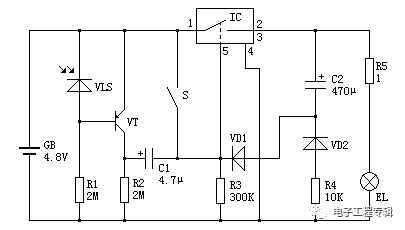
图25 自动应急ç¯ç”µè·¯å›¾è¯¥è‡ªåŠ¨åº”急ç¯ç”µè·¯ç”±å…‰æŽ§ç¯ç”µè·¯ã€ç”µå开关电路和延
RandM Tornado 9000 is a new Disposable Vape device It contains 18ml 5% nic salt e-juice and vape up to 9000 puffs. It's recharge, The rechargeable port at the bottom of the device guaranteeing you finish the last drop of the ejuice in the tank all the time. The price of the randm tornado 9000 is very good price, if you want to buy randm tornado 9000 near me, please contact us.
Tornado 9000 Puffs, RandM 9000, Randm Tornado 9000, 9000 puff disposable, 9000 Puffs vape
Shenzhen Kate Technology Co., Ltd. , https://www.katevape.com