This paper uses a single-chip microcomputer to realize wireless data transmission communication and real-time alarm function, and design a low-cost general-purpose ward call system. The whole system adopts wireless communication, which reduces the difficulty of complicated wiring, installation, maintenance and disassembly, and can monitor multiple wards and facilitate expansion and upgrade.
1 system design
This design uses a mode that separates the slave and the master. The slave is installed in each ward, and the host is installed in the infirmary or duty room. When multiple slaves are in the state of waiting for an external call signal, the master is in a state of waiting to receive the slave call information, and the wireless data is used between the slave and the host.
Transfer communication. When the patient presses the slave button installed on the bedside, the host installed at the nurse station sends a tone after receiving the signal, and the LED is illuminated, the digital tube displays the bed number and the number of calls to the patient, and the doctor or nurse displays according to the display. Bed number for treatment and service.
The hardware design of the ward call system mainly includes two parts: the host hardware design and the slave hardware design. Host hardware design includes RF chip
Peripheral circuit, display part, alarm part and simple peripheral circuit design of AT89C51 chip. The slave hardware design includes the design of the peripheral circuit of the RF chip, the external input circuit, and the simple peripheral circuit of the AT89C51 chip.
1.1 Host hardware circuit design
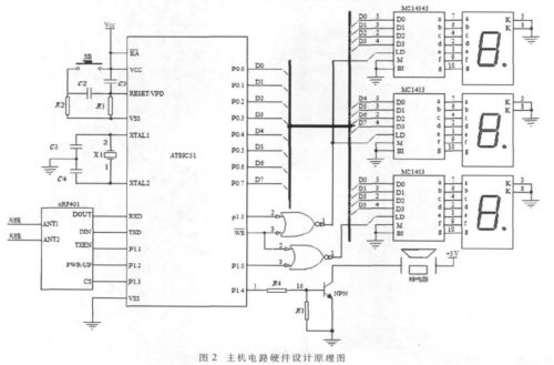
The system uses AT89C51 as the controller, and adopts the RF chip nRF401 to design the receiving/transmitting circuit to realize the data transmission with the slave [1]. When the nRF401 chip receives and processes the received data or the controller transmits and transmits information to the nRF401 chip, the communication between the nRF401 chip and the controller adopts the asynchronous serial communication method. In this communication mode, the RXD terminal and the TXD terminal of the microcontroller are respectively connected to the DOUT terminal and the DIN terminal of the nRF401 chip, and serve as a data serial transmission channel between the two. The P1.1 port is connected to the TXEN port of the nRF401 chip to select the working state (transmitting state or receiving state) of the nRF401 chip. The P1.2 port is connected to the PWR-UP port of the nRF401 chip to control the power saving state of the nRF401 chip. Port P1.3 is connected to the CS port of the nRF401 chip to select the transmit frequency of the nRF401 chip (the chip has two transmit frequencies).
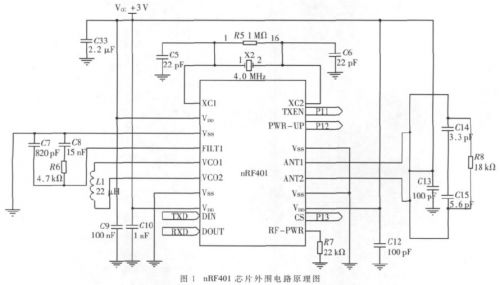
In addition, the ANT1 and ANT2 ports of the nRF401 chip are connected to the transmit antenna. The nRF401 peripheral circuit is shown in Figure 1. In order to facilitate the use of lower cost PCB antennas, the antenna interface in this design is designed as a differential antenna [2]. The hardware circuit design of the system host is shown in Figure 2.


1.2 slave hardware circuit design
A ward call system in this design has a host and multiple slaves to enable real-time calls from multiple wards to hosts installed in the medical staff's duty room. The peripheral circuit design of the slave controller, the connection mode of the RF chip nRF401 and the controller, and the design of its peripheral circuits are all consistent with the host. The difference is that the display and alarm hardware circuits are missing and an external request information receiving circuit is added. The external request information receiving circuit design in the slave only relies on a P0.0 port to wait for receiving an external high level. Once the SB2 is pressed, the LED is lit, and the P0.0 port is connected to the external high level, and the signal is quickly performed. The information is sent, and the call is automatically terminated until the transmission success message fed back by the host is received, and the state of waiting for the external request signal is continued.
2 system software design
In the process of software design, the anti-interference performance of system communication and the specific implementation method of normal communication identification must be considered, as well as the specific software implementation method for solving information collision.
2.1 host program design
The host program design mainly includes initialization program, data transmission program, receiving data program, delay program, LED display program and buzzer alarm program. These programs are not implemented as subroutines because the implementation of each function is not completely independent, but intertwined, making it difficult to implement the subroutine. In this design, the system function module program is written in the single-chip assembly language. The main program flow of the host is shown in Figure 3. 

Fork Type Connecting Terminals
Fork Type Connecting Terminals,Terminals,Connecting Terminals
Taixing Longyi Terminals Co.,Ltd. , https://www.longyiterminals.com