TL494 switching power supply circuit
Cars have begun to enter our homes, and high-performance car audio with superior performance is increasingly favored. In the past, 12V lead batteries were directly used for car audio, so that the pulses and other interference generated by car ignition directly became the main source of audio noise. The 12V low voltage single power supply also limits the audio output power, and the power amplifier circuit can only use the OTL circuit, which has poor frequency response characteristics. With the development of components and technology, the switching power supply has been fully applied to car audio. It can provide dual power supplies with higher voltage, and can suppress the intrusion of various noises. The power amplifier circuit also uses OCL circuits to make the car audio effect really up to the grade. The switching power supply for car audio applications meets the needs of technological development.
Figure 1 is a car audio switching power supply circuit, the circuit is mainly composed of two integrated circuits TL494 and KIA358, drive tube Q702 and Q703, switch tube M704 ~ M709, transformer, output rectifier and filter. TL494 is a pulse width modulation switching power supply integrated controller, its maximum drive current is 250mA, working frequency is 1 ~ 300kHz, the output mode can choose push-pull or single-ended form. The internal block diagram is shown in Figure 2. Refer to the TL494 pulse width modulation control circuit for details. It mainly consists of a triangular wave oscillator, two comparators CMP1 and CMP2, two error amplifiers A1 and A2, 5V reference voltage source, trigger and output driver.
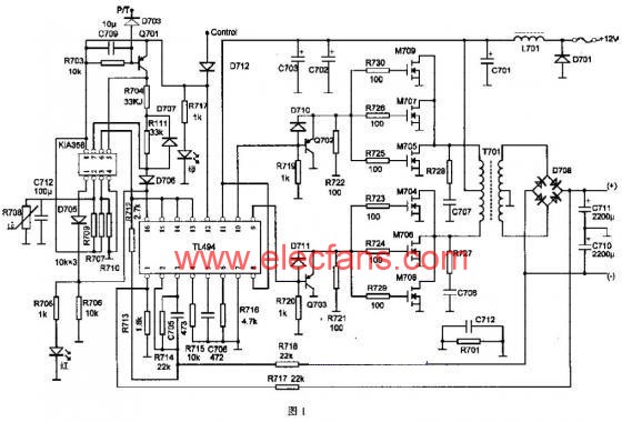

The triangle wave oscillation frequency is determined by the external connection of pins 5 and 6 Ct and Rt. The oscillation frequency fosc = 1.2 / Rt × Ct. The triangle wave oscillation signal is sent to the two comparators, namely the dead time comparator and the PWM comparator. The two comparators output to or Gate circuit. In this way, only when the amplitude of the oscillation signal level is higher than the dead time control level and the error input level at the same time, the output level of the OR gate is inverted. The pulse output is controlled by the trigger and the 13-pin output mode. When the 13-pin is connected to the low level, the internal trigger is disabled. The 13th pin of this circuit is connected to a high level (the reference voltage 5V is provided by the 14th pin), and the two output pulses are controlled by the triggers Q and Q, respectively, and the push-pull output through the two NOR gates and the push tube. 48%, the frequency is half of the triangle wave oscillation frequency. The dead time is set by the 4-pin voltage and the range is between 0 ~ 3.3V. The error amplifier A1 is used as the output voltage sampling error amplifier, and as a result, the pulse width is controlled by the PWM comparator to stabilize the output voltage. The error amplifier A2 is used for protection control. Pin 15 is connected to the reference voltage 5V (provided by pin 14), and pin 16 is the control input. During start-up protection, over-temperature or over-current protection, pin 16 is high, and at this time, the error amplifier A2 outputs a high level, which is higher than the amplitude of the triangular wave level of the oscillator, so that the driver has no drive pulse output , Safe load power failure.
The safety protection circuit is completed by the KIA358 circuit. When an abnormal situation occurs, it provides a high level to the 16 pins of TL494. KIA358 is a dual op amp circuit (see Figure 3).
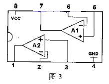
The op amp A1 is used for over-current protection, and pin 6 provides a reference voltage of 5V by pin 14 of TL494. Under normal circumstances, the P / T end is high, and pin 5 is low, so pin 7 outputs low, and pin 16 of TL494 is also low. When the P / T terminal detects a low level due to over-current or other reasons caused by the op amp, pin 5 is high and is higher than the reference level of pin 6, and pin 7 outputs a high level to protect the action. The op amp A2 is used for boot protection and overheat protection. The voltage of pin 3 of the non-inverting input terminal is obtained by dividing the control voltage 12V through two resistors R707 and R709. The voltage at the inverting input is divided by R710 and thermistor R708. The resistance value of R708 is about 100kΩ at normal temperature, the level of pin 2 is higher than that of pin 3, and pin 1 will output low level. When the temperature rises to nearly 100 ° C, the thermistor resistance drops below 10kΩ. The level of pin 2 is lower than the level of pin 3, the output is reversed, the protection action, and the red LED is on. Capacitor C712 is used for boot protection. At the moment of booting, C712 charges, so that the level of pin 2 is lower than the level of pin 3. At this time, the protection action is performed and the red LED lights up. When the C712 is fully charged, the level of pin 2 is higher than the level of pin 3, and pin 1 is turned to low level, the red light-emitting diode is extinguished, the protection is cancelled, and the work is normal, only the green light-emitting diode is on. The 14-pin reference voltage of TL494 is provided by the 12-pin. The 12-pin is connected to the car power lock through the diode D712. Only when the car unlocks the power lock, the 12 pin has the working voltage and the power supply works normally. The 9-pin and 10-pin outputs of TL494 are buffered by Q703 and Q702 to drive the field effect tube, then boosted by the transformer, and rectified and filtered to supply power to the audio in the form of a stable positive and negative power supply. The connection of Q702 and Q703 acting as a switch tube is without DC bias. When the output driving signals of pins 9 and 10 of TL494 are high, the signals are added to the gate of the FET via diodes D711 and D710, respectively, and Q703 and Q702 are reverse-biased. When the drive signal is low, Q703 and Q702 are turned on, and the charge accumulated in the gate capacitance of the FET is quickly discharged, turning off the FET.
In terms of component selection and circuit production, high frequency, large power supply, high efficiency, and the specific needs of car audio should be considered.
Switching power tube uses metal oxide field effect tube. Compared with bipolar transistor, power FET has many advantages:
1. The driving power is small and the driving circuit is simple, which can make the circuit structure compact and miniaturized;
2. The cutoff frequency is high, and there is no need to add reverse bias;
3. Simple parallel connection can be implemented;
4. No secondary breakdown;
5. There is no storage time;
6. There will be no thermal breakdown.
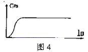
Since the battery power supply voltage is only 12V, the current value that can be tolerated by conduction is mainly considered. When the power is large, the switch tube should be connected in parallel with multiple tubes. After Vgs exceeds the turn-on threshold voltage, the ratio of drain current to gate voltage increases linearly. The rate of change of drain current to gate voltage, that is, transconductance Gfs is actually a constant when the drain current is large. It can be seen from the relationship between the transconductance Gfs and the drain current in FIG. 4 that the rise of transconductance increases the gain of the MOSFET in direct proportion to the increase of the drain current, which in turn increases the input capacitance. Therefore, The addition of a booster stage allows sufficient current to charge the input capacitor, reducing rise and fall times, and increasing the switching speed of the MOSFET. The driving stage has a low enough output impedance to avoid positive feedback oscillation of the circuit. In addition, MOSFETs are prone to oscillation when operating at high frequencies. Therefore, the length of the connection line with the MOSFET pins should be reduced as much as possible in the design of the circuit board, especially the length of the gate lead. Otherwise, a small resistor must be connected in series with the MOSFET pin, and the small resistor should be as close as possible to the gate of the tube. This circuit uses a 100Ω resistor connected in series with the gate, plus two sets of RC loops R728, C707 and R727, C708 to change the load curve of the MOSFET tube, and absorb excess energy to turn off the MOSFET, as a MOSFET switch protection circuit.
In the production of transformers, first of all, the magnetic core and its cross-sectional area S must be determined according to the output power, which mainly determines the efficiency of the switching power supply. It should be ensured that the transformer works in the linear region of the magnetization curve. And determine the maximum magnetic flux density Bmax, the best starting point is Bmax = Bsat / 2. Then select the wire according to the required power, and then determine the number of primary coil turns by N = V × 104 / 4f × Bmax × S, where f is the operating frequency and V is the operating voltage. And according to the secondary voltage required to determine the number of secondary coil turns.
Different audios require different voltage levels. The number of primary and secondary coils can be changed appropriately, as well as the resistance of sampling resistors R717 and R718 to obtain the appropriate voltage. The power rectifier cannot use ordinary rectifier diodes. Because the switching power supply works in a high-frequency state, the rectifier should use high-efficiency fast recovery diodes, ultra-fast recovery diodes or Schottky barrier rectifier diodes.
The output filter capacitor requires that the smaller the ESRmax value, the better. The ESRmax value directly affects the output ripple voltage. ESRmax = â–³ Iout / â–³ Vout, where Iout = 0.25Ii (Ii is the design output current). â–³ Vout is the peak-to-peak value of the allowable output ripple voltage. The minimum output capacitance can be derived from Cout = â–³ Iout / 8f â–³ Vout (where f is the operating frequency). The actual capacity should be much larger than Cout, because the filter capacitor capacity directly affects the low-frequency transient characteristics of the power amplifier.
The car audio switching power supply boosts a single 12V voltage and outputs a positive and negative power supply. Its working environment is low voltage, large current and high frequency. The production process mainly considers two issues of high current and high frequency. The printed board design must pay attention to the fact that there is no solder mask on the grounding part of the large current, so that the tin is thickened during the production, and the grounding area is large. The transformer pins working on the high current should pay attention to the welding process to prevent heat generation. Each heating device must have a good Heat dissipation. In the design of car audio switching power supply, only by paying attention to the selection of components and the wiring and manufacturing process of printed board to prevent unnecessary heat loss and self-oscillation, can we produce a high-quality switching power supply suitable for specific requirements.
This Computer Speaker is powered by USB interface on computers or laptops, plug and play, save energy. 3W output brings you high-quality clear binaural sound. Lightweight and portable design makes you can hold it with single hand, save space on the desk. Made of ABS and TPU, which makes this speaker durable and firm. Believe it is a great companion for your computer and laptop.

Usb Tiny Speakers,Usb Electric Speakers,Usb Powered Speakers,Mini Speaker Laptop
SHENZHEN HONK ELECTRONIC CO., LTD , https://www.honktech.com