The clock device design employs an I2C programmable fractional phase-locked loop (PLL) to meet high-performance timing demands, ensuring zero parts per million (PPM) synthesis error. High-performance clock integrated circuits (ICs) typically feature multiple clock outputs designed to drive various subsystems within applications like printers, scanners, and routers—such as processors, FPGAs, data converters, and more. These complex systems often require dynamic updates to the reference clock’s frequency to support multiple protocols like PCIe and Ethernet.
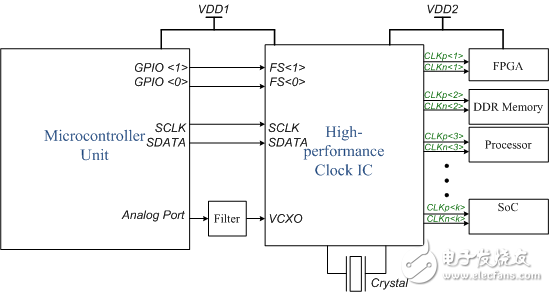
The clock IC operates as an I2C slave, requiring a host controller to configure its internal PLL logic. This control logic can be written directly to the microcontroller, which functions as an I2C master. Using this setup, the microcontroller configures the volatile memory on the clock IC and controls the PLL. Consequently, the system clock frequency can be dynamically updated through the on-board MCU-IC combination. Programmable microcontrollers offer control logic for high-performance clock ICs, simplifying overall designs and reducing costs by minimizing the number of on-board ICs and traces.
**Theory of Operation**
Figure 1 illustrates the basic PLL architecture for a high-performance clock device. This design employs a scaling factor for clock synthesis at the PLL output port. The formula for the final output frequency is:
\[ f_{OUT} = \frac{f_{REF} \times \left(\frac{DIV_N}{DIV_R}\right)}{DIV_O} \]
Where:
- \( f_{REF} \) represents the input reference crystal frequency (typically ranging from 8 MHz to 48 MHz).
- \( DIV_R \) (including \( DIV_R1 \) and \( DIV_R2 \)) is the division factor of the input reference frequency, known as the prescaler.
- \( DIV_N \) is the fractional-N factor.
- \( DIV_O \) (including \( DIV-O1, DIV-O2, DIV-O3, \) and \( DIV-O4 \)) is the post-divide factor before output.
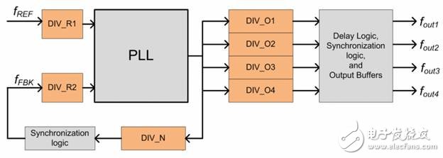
The orange blocks in Figure 1 represent programmable parameters, and the associated equations are fully programmable. These parameters can be written to the non-volatile memory of the clock device during manufacturing. The clock device contains both volatile and non-volatile memory, which copies their contents to each other upon power-up. The non-volatile memory is pre-written with the desired configuration at the factory. When powered on, the contents of the non-volatile memory are copied to the volatile memory, and the PLL generates the necessary default clock outputs.
One key feature of the clock IC is runtime programming via the I2C interface. This allows users to modify the volatile memory contents for immediate adjustments. Users can implement instant programming of their preferred profiles through the host controller using appropriate I2C instructions.
The device’s non-volatile memory can also store predefined multi-user configurations. Users can select one of these configurations using the Frequency Select (FS) function. The FS-pin is a CMOS input pin available in the device, which uses an N-bit external CMOS signal to internally select a configuration file stored in non-volatile memory. This selected configuration is copied to volatile memory, and the PLL outputs a different signal.
At the same time, the microcontroller communicates with the high-frequency clock through I2C, providing essential data. The advantages of using a microcontroller include its diverse communication peripherals and protocols, such as I2C, SPI, UART, Bluetooth, and ZigBee. This enables the system to transfer data to other microcontrollers in a master-slave configuration or to custom apps on Android and iOS devices. Additionally, microcontrollers come with numerous IDE tools, simplifying the design process. This supports the use of I2C instructions to configure PLL parameters and develop custom applications.
**High-Performance Clock Application Requirements**
High-performance clock ICs are tailored for consumer, industrial, and networking applications. These ICs feature multiple differential and single-ended outputs derived from different PLLs, all programmable via the I2C interface. They also support reference clocks for critical interface standards such as PCI Express (PCIe) 1.0/2.0/3.0, USB 2.0/3.0, and 10 Gigabit Ethernet (GbE). Additional features like Voltage-Controlled Crystal Oscillators (VCXOs) and Frequency Selection (FS) are also supported.
The high-performance clock IC is designed to operate in I2C slave mode, necessitating an on-board I2C host to control several programmable features:
- In-system programming via the I2C interface
- Configuration updates via the FS pin
- External reset operation
- Voltage-Controlled Crystal Oscillator (VCXO) operation
**Role of Microcontrollers in Clock IC PLL Control**
Connect the clock IC to the microcontroller circuit as shown in Figure 2. The clock IC includes an internal PLL block designed to produce a tuning voltage (Vtune) as a fixed DC voltage, varying according to the frequency band. The PLL module accepts the local oscillator frequency at its input and amplifies it through an internal preamplifier. Additionally, the prescaler downconverts the input frequency and passes it to the phase comparator.
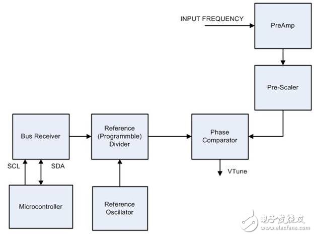
The microcontroller sends data to the programmable divider via I2C. The divider also receives input from a reference oscillator like a 4 MHz crystal oscillator. The phase comparator (or phase detector) receives the local oscillator frequency (e.g., 87.15 MHz) through the prescaler and compares it to the input from the microcontroller (e.g., 87.15 MHz) referenced to the divider and reference oscillator. If both inputs match, the phase comparator generates the Vtune tuning voltage. Any slight mismatch between the local oscillator frequency and the microcontroller frequency data results in no tuning voltage or output. Figure 3 shows the complete block diagram.
With the help of a microcontroller, the PLL forms a closed loop by tuning the local oscillator frequency and producing a tuning voltage at the output. This tuning voltage increases as the frequency moves from the lower channels to the higher ones. The microcontroller can adjust the step size by altering the values of the prescaler and the programmable divider.
Step Size = (Local Oscillator Frequency / Prescaler) × (Programmable Frequency Divider / Reference Oscillator)
**In-System Programming via the I2C Interface**
In-system programming allows for rapid and efficient system design iterations. The programming data sequence can be transferred to the clock device via the SCL and SDA pins, with the sequence of operations programmed into the on-board microcontroller (as master) to interact with the slave clock at runtime using commands and data.
For instance, consider a system where the clock signal must be a multiple of the sample rate, varying between 155.52 MHz and 156.25 MHz. This means the clock driving the serial controller must flexibly switch between these two values. The microcontroller master can access and modify the PLL configuration written to the volatile memory to meet these frequency requirements.
**Update Configuration via Frequency Selection (FS) Pin**
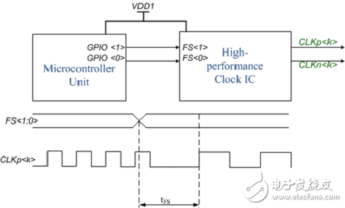
High-performance clock devices support multiple user profiles with personalized configurations. Regarding FS pin transitions, high-performance clock devices have two timing specifications—fast switching and slow switching.
Fast switching is available for output ON/OFF, output crossover value changes, and output MUX setting changes. Slow switching is useful for changing PLL parameters (including PLL ON/OFF). As the names suggest, output changes occur faster in fast switching compared to slow switching. Both switch types can turn the output on or off without introducing errors. Figure 4 demonstrates the timing relationship between FS and the output clock.
**External Reset Operation**
When an external reset is active, the clock IC enters a low-power mode. The output and I2C bus signals are in a high-impedance (HI-Z) state until the external reset is canceled and initialization is complete. The external reset restarts the volatile memory contents, copying the configuration stored in non-volatile memory to volatile memory. This feature is useful when reinitializing an application running on any system.
**Voltage-Controlled Crystal Oscillator (VCXO) Operation**
For certain applications, the output clock frequency should track the input data stream using analog feedback. As shown in Figure 5, the clock IC is part of a larger phase-locked loop. The ASIC or SoC tracks the input stream, calculates the error, and generates a PWM signal (usually), then feeds back the error information to the local clock generator for frequency tuning.
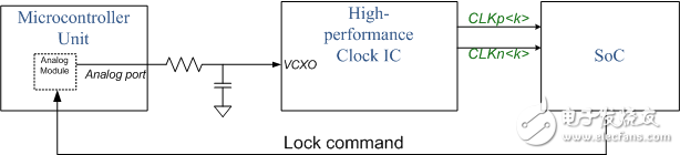
The VCXO function modifies the PLL frequency so the frequency pull does not depend on crystal characteristics, temperature, voltage, or device process. VCXO modulation is linear and precise. A clock reference can also be used. With the built-in analog module of the microcontroller, the VCXO's control logic is accurate to six decimal places.
As an I2C master, the microcontroller configures the internal volatile memory of the clock IC and controls the PLL. Thus, dynamic updates to the system clock frequency can be achieved through the on-board MCU-IC combination. Developers can use programmable microcontrollers to provide control logic for high-performance clock ICs, reducing the need for on-board ICs and traces, making the overall system design more compact.
The microcontroller is equipped with powerful IDE tools to accelerate application development. Integrated Programmable System-on-Chip (PSoC) devices further simplify design and help reduce overall product costs.
Solar Panel Grounding Wire Size,Solar Grounding Wire Size,Solar Panel Ground Wire,Pv Grounding Wire
Sowell Electric CO., LTD. , https://www.sowellsolar.com