Related application notes: Intel (R) T1 / E1 / J1, N + 1 Redundancy With Analog Switches and Intel (R) LXT38x Line Interface Units
Table 1. Comparison of analog switches and relays
| Relay | Analog Switch | |
| Board Space | 100mm2 | 15mm2 |
| Power ConsumpTIon | 140mW | 5µW |
| Switching Speed | 4ms | 30ns |
| Reliability | Mechanical OperaTIon | No Moving Parts |
This application note describes how to use analog switches to implement T1 / E1 / J1, N + 1 redundancy protection. It also provides some guidelines for selecting analog switches and gives test results using Maxim / Dallas analog switches and T1 / E1 / J1 transceivers.
Redundant structure Figure 1 and Figure 2 are two redundant structures using analog switches. For clarity, the sending interface and the receiving interface are drawn separately. For each T1 / E1 port, the receiving and sending interfaces are on the same circuit board. The figure shows typical interface transformers and resistors recommended for Dallas / Maxim transceivers (such as DS2155). In both structures, there is a protection bus walking on the backplane, and input and output signals can be sent to the analog switch through this bus. The protection bus is directly connected to the standby (protection) line card.In Figure 1 ("Structure A"), the analog switch is located on the line card. The advantage of structure A is that it does not require a separate line card for protection switching as in "structure B" below. However, it requires that the switch be able to obtain power even during failover, which requires a separate dedicated power supply.
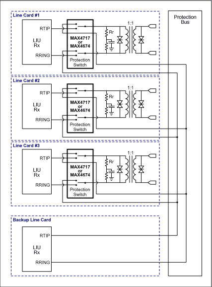
Figure 1a. Redundancy structure A: receiving channel.
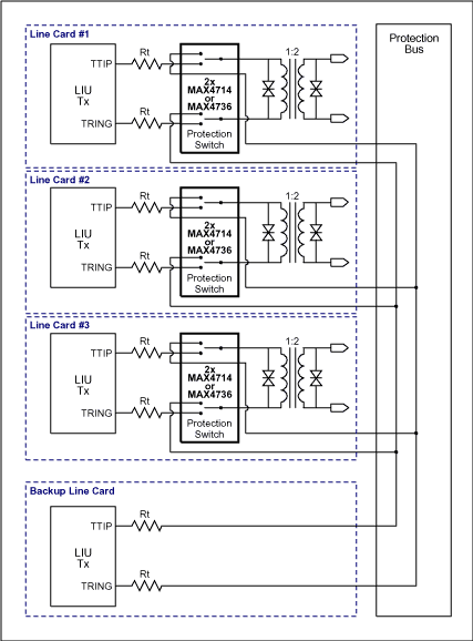
Figure 1b. Redundancy structure A: transmit channel.
In Figure 2 ("Structure B"), the analog switch is in a separate "Protection Switch Card". The advantage of structure B is that it does not depend on the normally "on" power supply in the line card, but it requires additional protection switching cards.
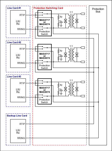
Figure 2a. Redundancy structure B: receiving channel.
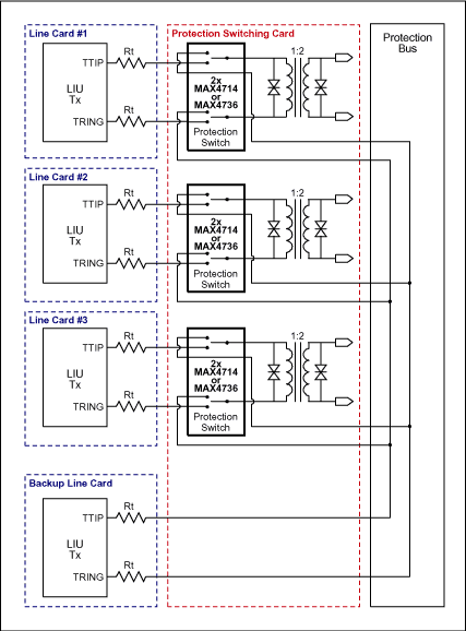
Figure 2b. Redundancy structure B: send channel.
In order to meet the T1 / E1 / J1 interface specification, the selection of an analog switch must carefully consider its electrical characteristics. Because the requirements for the sending and receiving ports are very different, we examine them separately.
Transmit interface switch On the transmit interface, the on-resistance (Ron) of the switch is a very important parameter. In Figure 1 and Figure 2, we can see that the Ron of the switch is in series with the output driver and the primary coil of the transformer, so it will slightly reduce the amplitude of the output pulse. In most cases, the reduction in amplitude can be compensated simply by reducing the series resistance (Rt), which can correspond to the typical Ron of the switch. For example, if the transceiver recommended Rt is 11Ω and Ron (typical) is 0.5Ω, then the actual Rt should be 10.5Ω. To ensure correct operation over the entire operating range (including changes in temperature and power supply), it is important to keep Ron well below Rt resistance. Lower Ron will also have better Ron flatness, thereby reducing the distortion of the output pulse.Some transceivers (such as the DS2155) allow software to adjust the amplitude of the output pulse. This is very useful for transceivers that do not use output resistance (Rt = 0) to ensure sufficient pulse mask margin.
Another important parameter in the transmission interface is the switch on and off capacitance (CON and COFF). Excessive on-capacitance will distort the output pulse and reduce the return loss characteristics of the transmitter. The shutdown capacitor has an important effect when the standby line card is sent through the protection bus, as shown in Figure 1 and Figure 2. In this case, the capacitance seen by the output driver is the parallel connection of the shutdown capacitors on all other line cards.
The excellent performance of analog switches such as MAX4714 and MAX4736 is very suitable for T1 / E1 transmission switching. They have very low Ron (typical 0.6Ω) and very low capacitance (typical CON = 65pF, COFF = 30pF).
The main problem that needs to be considered when the receiving interface switch is in the receiving channel is the impact of the switch on the line terminal matching, and therefore the performance of the received return loss. The reception return loss is directly related to the matching between the input terminal and the rated line impedance in the relevant frequency range. In T1 / E1 / J1 applications, this frequency range extends to 3 MHz. Therefore, low capacitance is very important to maintain high-frequency performance in compliance with standards such as ITU-T G.703. Another advantage of low capacitance is that it can help improve the switch off isolation. Shutdown isolation is particularly important in the receiving interface, which directly affects noise coupling and bit error rate.The switch Ron resistor will be connected in series with the receiver pin (RTIP / RRING), as shown in Figure 1 and Figure 2. If the termination of the line is provided solely by the external resistor Rr, because the receiver impedance is very high, Ron will not cause a great impact on the receiving circuit. However, some modern transceivers such as the Dallas DS2155 provide internal termination by connecting a software-selectable resistor in parallel with an external resistor Rr (60Ω each). Therefore, the Ron of the receiving interface can be larger than that of the transmitting interface (in order to reduce the capacitance), but it should still be kept small enough so as not to affect the performance of the internal receiver.
Maxim's MAX4717 provides well-balanced Ron and low capacitance, and is particularly suitable for T1 / E1 / J1 receiver interface applications. It has a typical Ron of 3Ω and has a very low capacitance (typical values ​​CON = 15pF, COFF = 9pF).
Implemented with Dallas / Maxim DS2155Test the circuit of Figure 1 and Figure 2 with the evaluation board of the Dallas DS2155 single-chip transceiver. The analog switch uses a 3.3V power supply. The values ​​of the components in the test device are shown in the following table:
| Component | Value T1 Mode | Value E1 Mode (Twisted Pair) | Value E1 Mode (Coaxial Cable) | Notes |
| Transmit Transformer | 1: 2 PE-65771 | 1: 2 PE-65771 | 1: 2 PE-65771 | Can also use other Dallas / Maxim recommended transformers (See App Note 351: "Transformer SelecTIon Guide") |
| Receive Transformer | 1: 1 PE-68644 | 1: 1 PE-68644 | 1: 1 PE-68644 | |
| Rt | 0Ω | 10Ω | 10Ω | Internal transmit termination off |
| Rr | 60Ω | 60Ω | 60Ω | Internal receive termination on |
| Cr | 0.1μF | 0.1μF | 0.1μF | |
| Receive Switch | MAX4717 | |||
| Transmit Switch | MAX4714 | |||
When using this circuit, the internal transmit termination function must be turned off. In order to use the same transmission resistance in E1 twisted pair and coaxial cable, the following values ​​must be written to the transmission line compensation control register (TLBC):
TLBC (Address 7Dh) = 6Ah
It sets the voltage of the driver so that the output pulse has the correct amplitude on both 120Ω (twisted pair) and 75Ω (coaxial) loads.
According to the actual application, you also need to add surge protection devices to the circuits in Figure 1 and Figure 2. For more information about surge protection, please visit the relevant application notes on the Dallas / Maxim website.
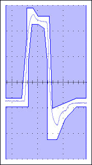
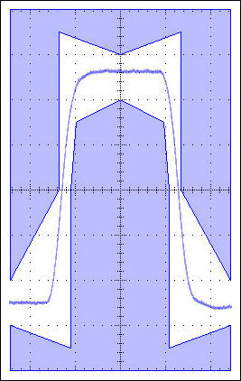
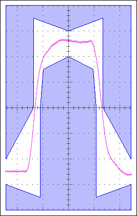
Test results According to Figure 1 and Figure 2, we can see that when the number N of circuit boards in the N + 1 redundant structure increases, the maximum parallel shutdown capacitance seen by the transceiver of the standby board also increases accordingly. This parallel capacitor will affect the shape of the output pulse and the return loss characteristics. On the other hand, under normal working conditions (the standby board is not working), the on-capacitance of the switch is the most important capacitance seen by the transceiver, and this (smaller) capacitance is easier to handle.In order to achieve good performance under the worst-case capacitive load (the standby board is activated), it is recommended that N should not exceed 8 (1: 8 redundancy protection). Figures 3 to 5 show the measured T1 / E1 output pulses.
Figure 3. Output pulse, T1 mode
| T1, 0-133ft LBO, 0 ft cable, working normally (1) | T1, 0-133ft LBO, 0 ft cable, N = 8 (2) |
 (1) Output pulse after passing through two series switches on the transmission channel (1) Output pulse after passing through two series switches on the transmission channel |  (2) The output pulse of the spare board in the 8 + 1 structure (2) The output pulse of the spare board in the 8 + 1 structure |
Figure 4. Output pulse, E1 twisted pair
| E1, coaxial cable, working normally (1) | E1, coaxial cable, N = 8 (2) |
 (1) Output pulse after passing through two series switches on the transmission channel (1) Output pulse after passing through two series switches on the transmission channel | 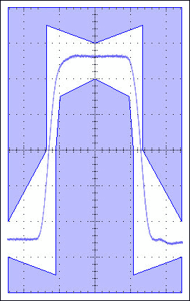 (2) The output pulse of the spare board in the 8 + 1 structure (2) The output pulse of the spare board in the 8 + 1 structure |
Figure 5. Output pulse, E1 coaxial cable
| E1, twisted pair, working normally (1) | E1, twisted pair, N = 8 (2) |
 (1) Output pulse after passing through two series switches on the transmission channel (1) Output pulse after passing through two series switches on the transmission channel | 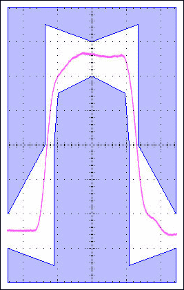 (2) The output pulse of the spare board in the 8 + 1 structure (2) The output pulse of the spare board in the 8 + 1 structure |
Universal Series Extension Sockets
Socket Extension,Trailing Socket,Plug Socket Extension,Single Socket Extension Lead
Heikki Technology Co., Ltd. , https://www.heikkipower.com