A Silicon Bipolar Broadband PLL Building Block Integrated Circuit
Abstract: A broadband phase-lock loop (PLL) building block integrated circuit (IC) that can accommodate signal frequencies from 0.5GHz to 9GHz is presented. The design integrates a prescaler with selectable divide raTIo, a phase detector, a voltage-controlled oscillator for producTIon tesTIng, and associated circuitry. The chip is designed on Maxim's GST-2 bipolar linear array technology and is packaged in a 16-pin plasTIc dual in-line package. The result is a low-cost, broadband solution for a variety of PLL systems.
© 1997 IEEE. Reprinted, with permission, Proceedings of the 1997 Bipolar / BiCMOS Circuits and Technology Meeting (BCTM); September 28-30, 1997.
The development focus for many high-speed PLL designs is evolving from research to economic challenges. System designers are calling for highly integrated, price-competitive solutions. A low-cost solution often requires the use of an inexpensive plastic package despite its detrimental effect on high-speed performance. A higher level of integration results in greater power dissipation, further increasing the challenges associated with a plastic package. Thus, the goal of the PLL building block described in this paper was to achieve broadband performance with low power dissipation and have the performance minimally affected by package limitations.
The PLL building block IC can accommodate an input signal frequency range from 0.5GHz to 9GHz making it effective for most PLL applications such as satellite communication systems, high-speed measuring equipment, and RF data communications. The chip was fabricated in a silicon bipolar technology , with NPN transistor fT and fmax equal to 24GHz and 22GHz, respectively. To improve the time-to-market, a linear array was used. The linear array is analogous to a gate array except that, instead of having pre-placed gates for digital functions, the linear array has pre-placed elements such as transistors, resistors, and capacitors for analog designs. A faster turnaround time may be achieved using a linear array, but increased layout parasitics and a fixed number of elements and element values ​​can prevent the designer from achieving an optimum design. Despite these potential limitations, broadband performance was still achieved through careful layout and creative designs, which used the availab le components most effectively.
A block diagram of the chip is shown in Figure 1. The chip receives a modulated signal from an external source within the 0.5GHz to 9GHz frequency range. The signal is phase-locked to an external RF input with an on-chip phase detector and off-chip loop filter. The prescaler is divided into two sections: a divide-by-eight block and a divide-by-eight / nine block. The VCO, charge pump, and loop filter were left off-chip so that the building block could be used in a variety of system applications. 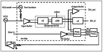
Figure 1. PLL building block and complete PLL circuitry.
The flip-flops in the divide-by-eight use a master / slave configuration with the Q-bar output fed back to the data input to divide the clock frequency by a factor of two. A schematic of the first flip-flop in the divide-by-eight chain is shown in Figure 2. A special feature of the first flip-flop is the inclusion of currents referred to as "keep-alive" currents and denoted IK in the schematic. Keep-alive currents reduce the time to fully switch Q9-Q16 by keeping the transistors from turning off. Values ​​on the order of 1/10 the main differential-pair current (ID) were used. All eight emitter-followers (Q1-Q8) were necessary for the first flip- flop in the divide-by-eight since the low output impedance and high current-drive capability of the emitter-followers increase the toggle rate. For following stages when speed was not a concern, the emitter-followers were eliminated (or reduced in number ) and the differential-pair currents were reduced to minimize power dissipation. 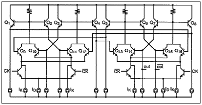
Figure 2. Schematic of first flip-flop in divide-by-eight chain.
The phase detector in this work is based on a standard design. A block diagram of the phase detector is shown in Figure 3. There are three outputs of the phase detector: UP, DWN, and LD. When the loop is out of lock, an irregular pulse train appears on either the UP or DWN outputs depending on whether the input signal frequency is faster or slower than the reference frequency. The filtered output of the other signal remains high. If the signal frequency and reference frequency are equal, the output pulse train is periodic and the average value a measure of the phase offset. 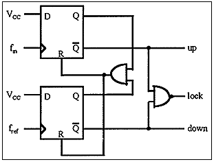
Figure 3. Phase detector block diagram.
The development of low-cost "at-speed" testing of the PLL building block is key to its success in production. An on-chip, high-frequency (~ 5GHz) ring oscillator is included. The purpose of the oscillator is to provide a method to test the frequency dividers during near-speed wafer or package testing. The VCO is a ring oscillator that uses interpolation to increase the frequency response [1]. The oscillator is powered separately through an external "enable" pin that disables its operation when grounded and allows operation when tied to the supply. The divide-by-two circuitry is used to reduce the test output signal to a frequency compatible with low-speed wafer testing and die-sorting.
Successful operation of the PLL building block IC at high-frequencies required careful re-design of the plastic package as shown in Figure 4. Ground inductance was required to be absolutely minimized to achieve good phase noise response. The high-frequency prescaler input (VRF ) was required to be well isolated from the phase detector input (REFIN). Six of the 16 pins on the SOIC package are ground pins and they are shorted to the paddle. The retooling provides a relatively "clean" ground point for the chip grounds and chip substrate to be connected. Surrounding the high frequency input signal with four of the ground pins (two on each side) improved the isolation of the input signal. Furthermore, retooling the package helped significantly improve the thermal resistance. The Φja of the package was reduced from ~ 100 ° C / W to 72 ° C / W and the maximum junction temperature of the chip under all cases never exceeds 125 ° C. 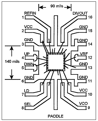
Figure 4. Package drawing.
Based on the physical characteristics of the package, a lumped parameter package model was developed. Figure 5 shows the model, with specific parameter values ​​that were used for simulation. (The values ​​given are for the shortest lead lengths.) The high-frequency input signal was placed in the center of the package to minimize bond wire and lead inductance, resulting in lower coupling and improved matching. 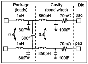
Figure 5. Package model.
The minimum detectable input signal versus input frequency for the packaged PLL building block is shown in Figure 6. An input signal of -20dBm or less is sufficient for operation over a broad range of frequencies. The design functions from 0.5GHz to 9GHz but requires slightly larger input power levels at the frequency bounds. Measurements of the packaged die were taken over a range of temperatures (-35 ° C to + 90 ° C). At lower temperatures, the PLL building block functions at higher speeds for a given input signal level because the transistor fT increases for decreasing junction temperatures. Simulation results predict the effects of temperature on performance. At each temperature the supply was varied from 4.5V to 5.5V. The data in Figure 6 shows that the performance of the circuit is relatively independent of supply voltage. 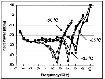
Figure 6. Divider Sensitivity of packaged devices over various supply voltages and temperatures.
Divider sensitivity was also measured for the unpackaged die using a membrane probe. The similarity of the two curves shown in Figure 7 demonstrates the broadband performance of the package. There is little difference between wafer and package measurements up to 9GHz. 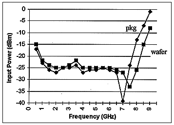
Figure 7. Divider Sensitivity: comparison of package and wafer probe data under nominal conditions. (T = 25 ° C, VCC = 11V)
The input buffer driving the divider is designed to match to a 50Ω impedance. The measured results of S11 shown in Figure 8 can be explained with an understanding of the input buffer topology. The impedance match is achieved through a 50Ω internal resistor connected between the input and a bias voltage. At very low frequencies, the impedance of the bias circuitry increases the input impedance. Capacitance at the bias node lowers the impedance of the bias circuitry as the frequency increases. A good match is achieved mid-band. At high frequencies , package and layout parasitics begin to degrade the input impedance. The data shown also reflects the impedance of an SMA connector which further degrades performance at high frequencies. Better than -5dB for S11 can be achieved over the full band of operating frequencies which is adequate for most closed-loop applications. 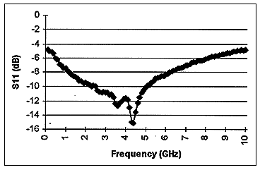
Figure 8. Input impedance of packaged PLL building block.
The oscillation frequency of the on-chip oscillator used for test purposes is approximately 5GHz. The design was not optimized for speed and higher frequencies can be achieved with this design. The measured phase noise is -69dBc / Hz at an offset frequency of 100kHz.
The phase detector functions properly over the entire range of the divider. The outputs are open collector with external loading. With 150Ω loads, the output voltage on the UP and DWN pins is 1.1V. The LD output achieves a 2V swing when loaded with a 500Ω resistor. The minimum reference input signal required is -18dBm (matched to 50Ω) and can tolerate as much as + 10dBm.
The circuit die size is 70 mil x 75 mil. Roughly 85% of the linear array was utilized for the design of the PLL building block. Power dissipation under nominal conditions (T = 25 ° C and VCC = 5V) is approximately 500mW.
The design described in this paper is a broadband PLL building block capable of accommodating signal frequencies ranging from 0.5GHz to 9GHz. The manufactured part exemplifies a low-cost, fast time-to-market, design without sacrificing performance. This chip overcomes design problems associated with inexpensive packaging through effective package modeling, built-in testing, and retooling.
The authors wish to thank Larry Blue, Tom Jackson, and Steve Rosenbaum from Hughes Network Systems and Will Grimes from Maxim Integrated Products for their help in the development of the PLL Building Block.
References B. Razavi and JJ Sung, "A 6 GHz 60mW BiCMOS Phase-Locked Loop", IEEE Journal of Solid-State Circuits, Vol. 29, pp. 1560-1565, Dec. 1994.POLYBAG CANDLES TEALIGHT CANDLES IS IS POPULAR PACKING WAY IN ISREAL ,AND EUROPEAN COUNTIES .
THE DESIGN HAVE MANY COLOR AND PICTURE AS CLIENT CHOOSE .AND ASLO CHEAPER THAN BOX PACKING
TEALIGHT CANDLES HAVE 9-14GRAM PER PIECE .AND DIFFERNT BURNING TIME .
ANY INQUIRE PLS BE FREE TO CONTACT WITH ME
ANGEL YANG
Tealight Candle Polybag Packing
Tealight Candle Polybag Packing,Tealight Candle Storage Box Packaging,Tealight Candle Plastic Bag Packing,Polybag Pack White Tealight Candle
Shijiazhuang Zhongya Candle Co,. Ltd. , https://www.zycandlefactory.com