RFID (Radio Frequency Identification) technology is an automatic identification technology that matured from the 1980s and has developed rapidly in recent years. The technology covers a wide range of applications, and many of the automatic identification technologies in use can be attributed to RFID technology, but their working principle, operating frequency, technical characteristics, applicable fields and standards are different. The operating frequency of the RFID system mainly includes multiple frequency bands such as 125KHz, 13.56MHz, 400MHz, 860-960MHz, 2.45GHz, and 5.8GHz.
However, the allocation of frequencies and the maximum transmit power are different for different countries and regions. In some areas, RFID products in certain frequency bands may be banned. Among them, 13.56MHz RFID international standards are ISO14443 and ISO15693.
ISO14443 is divided into Type A and Type B. Type A is represented by Philips' Mifare one, and Type B is representative of the * currently being issued in China. ISO14443 is a near-coupling communication protocol with a communication distance of less than 10cm. ISO15693 is a loosely coupled communication protocol with a communication distance of 1.5m.
In the ISO15693 protocol, in order to transfer data from the reader to the loosely coupled IC card, not only 10% ASK modulation but also 100% ASK is used. In addition, there are two different encoding methods: one is "256" Take 1 in the middle, and the other is "1 in 1".
This part of the circuit was simulated by the Cadence spectre simulation environment and verified by SMIC CMOS 0.18um one play four metal process.
This RFID technology uses a unique new RFID chip technology. Unlike conventional RFID chips, this RFID does not use traditional EEPROM memory, but uses the memory technology - XPMTM (Super Permanent Memory) technology invented by Dr. Peng Zezhong. XPMTM, Super Permanent Memory. Called X-RFID, X-RFID features high security, low price, high reliability and large capacity. It can be widely used in library management, document security, attraction tickets, product anti-counterfeiting, e-wallet, asset management, Single product management, logistics and supply chain management and many other fields.
This article focuses on the design of the high-frequency analog interface module for the X-RFID chip. Sections 2 and 3 below describe the overall system architecture of the RFID chip. The fourth section describes the inductive coupling simulation model and simulation results of the 13.56MHz RFID system. Section V draws conclusions.
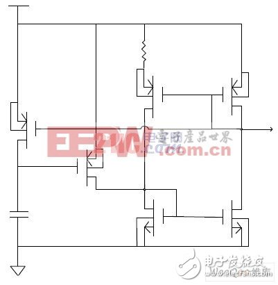
2. The working principle and system structure of the transponder chip13.56MHz RFID system structure conforming to the ISO15693 protocol standard is shown in the figure. This chip is used to obtain the power required for chip operation through inductive coupling, so it is called passive RFID chip. The main structure includes: analog front-end interface circuit, digital Logic control circuit and Memory circuit. This chip has only 2 PADs connected to the external antenna. The analog front-end interface circuit includes: full-wave bridge rectifier circuit, voltage regulator circuit, high-voltage protection circuit, modulation circuit, demodulation circuit, power-on reset circuit, Clock extraction circuit.
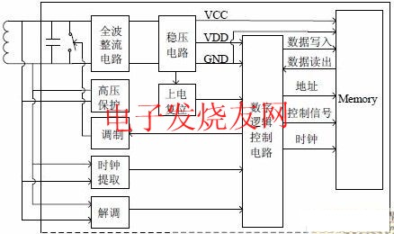
When the RFID tag chip enters the magnetic field of the card reader, the 13.56 Mhz AC sine wave signal is transmitted to the full-wave bridge rectifier circuit through the coupling between the antenna of the RFID tag chip and the reader antenna, and then converted into a full-wave bridge rectifier circuit. The DC voltage is regulated by the voltage regulator circuit to the required voltage value for the digital logic control circuit and the Memory circuit to be used as a power source.
Because the magnetic field strength emitted by the card reader is related to the distance between the card reader and the card reader, the magnetic field strength is large near the card reader, and the magnetic field strength is small when the card reader is far away. When the RFID tag chip is out of the card When the machine distance is very close, due to the high magnetic field strength, the voltage value coupled to the two ends of the RFID tag chip antenna is very high. If the high voltage protection is not applied, the internal circuit of the RFID tag chip will be damaged, so the high voltage protection circuit is indispensable. . The communication between the card reader and the RFID tag is a half-duplex mode. The commands sent by the card reader are superimposed on the carrier by ASK modulation and sent to the RFID tag chip. The RFID tag chip solves the command through its internal demodulation circuit. The call is sent to the digital logic control circuit for decoding, and then the corresponding instructions are processed. The data of the RFID tag chip is returned to the card reader by superimposing the data on the carrier sent by the card reader through the internal modulation circuit, and the card reader demodulates the data through the demodulation circuit of the internal wave. This way the reader and the RFID tag communicate with each other.
2.1 full wave bridge rectifier circuit
The full-wave bridge rectifier circuit replaces the 13.56MHz sine wave signal coupled by the antenna into a DC signal, and supplies it to the VDD and GND of the digital logic control circuit and the Memory circuit through the voltage stabilization circuit. The circuit diagram is shown in Figure 2.
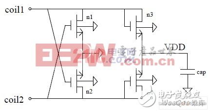
In the figure, two NMOS transistors in n1 and n2 are connected to the GND as a switching source, and the drain is connected to both ends of the antenna. The two NMOS transistors in n3 and n4 are used as diodes, the gate and the drain are connected together to one end of the antenna, the source is connected to the power supply VDD, and VDD is grounded through a large capacitor, which is a storage capacitor, that is, a storage antenna. The coupled charge is supplied to the internal circuit as the power supply VDD.
Where: Vm is the peak-to-peak value of the antenna sine wave signal, and Vth is the threshold voltage of the NMOS transistor.
2.2 clock generation circuit
The clock generation circuit is shown in Figure 3. The two inverter circuits form the latch circuit. The 13.56MHz sinusoidal signal with the opposite phase of the signal is applied to the NMOS transistors M7 and M8 through the antenna terminals coil1 and coil2. When the coil1 is high level, the coil2 is a low level signal. At this time, the NMOS transistor M7 is turned on, M8. Deadline. When coil1 is low, coil2 goes high, which is the NMOS transistor M7 is turned off and M8 is turned on. Through this alternate control, the clock generation circuit produces a 13.56 MHz square wave clock signal.
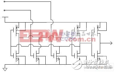
2.3 Bias generation circuit
The bias generation circuit is shown in Figure 4. The PMOS transistors M1 and M2 and the capacitor CAP form the startup circuit of the bias circuit. PMOS transistors M3 and M4, as well as NMOS transistors M5 and M6, and resistor R form a current offset independent of the supply voltage.
Since the width to length ratio of the M3 transistor is N times that of M4, and because of the width to length ratio of M5 and M6, the current I5 flowing through the M5 tube and the current I6 flowing through the M6 ​​tube are equal according to the principle of the current mirror. and
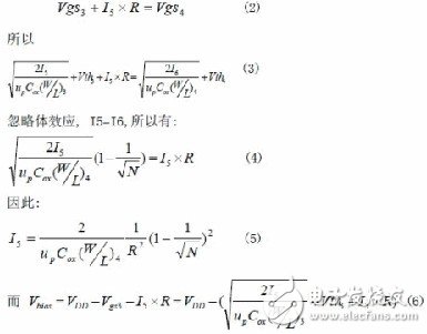
Since the above equations are constant, we can get a bias voltage Vbias that has a fixed difference from the power supply voltage VDD.
2.4 high voltage protection circuit
The high voltage protection circuit is shown in the figure. The high voltage protection circuit is very important in the RFID tag chip because the RFID tag antenna is very close when the magnetic field strength of the card reader is large and the RFID tag chip is close to the reader antenna. The voltage induced by both coil1 and coil2 can reach hundreds of volts. If the high voltage protection circuit is not applied, the device inside the chip will be damaged.
When the voltage induced by coil1 and coil2 passes through the rectifier circuit, if the output voltage is greater than the voltage drop of M3, M4, M5, M6 and R2, the voltage of coil1 and coil2 is limited. This protects the voltage across the coil1 and coil2 from the normal range.
2.5 voltage regulator circuit
The voltage regulator circuit is shown in the figure. In the RFID tag chip, a larger capacitor is needed to store enough charge for the tag to be used as a power source when the input energy is weak. If the input voltage is too high, the power supply voltage rises to a certain extent, the escaping circuit in the voltage regulator circuit will work, and the excess charge on the capacitor is released to achieve the purpose of voltage regulation. The regulator circuit in Figure 6 uses five PNP transistors. This regulator circuit achieves voltage regulation with a minimum of devices. Since the Vbe voltage of the PNP is around 0.7v, the regulation of the five triodes is around 3.5v. When the voltage exceeds 3.5V, the current will pass through the path from the emitter to the collector of the PNP to release the charge. Very good for the effect of pressure limiting.
2.6 modulation circuit
The modulation circuit is shown in the figure. MOD_DATA is the modulated data signal of the digital logic output. It is used to control the on and off of the M5 tube and the M6 ​​tube. This changes the strength of the parallel resonant circuit damping at both ends of the antenna, and realizes the amplitude modulation function. It completes the RFID tag to the card reader. Data transfer.
3. Circuit simulation resultsFrom the simulation results of the figure: In the 10% and 100% ASK modulation modes, the circuit can correctly demodulate the instructions from the correct reader and generate a 20us POR signal. At that time, the circuit's modulator function is correct, and can generate more than 10% ASK modulation on the antenna, so that the returned data can be received by the reader. The figure is the data of the tag return data and the waveform of the antenna.
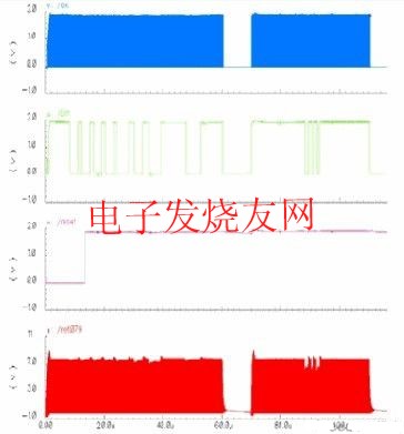
100% and 10% ASK modulation simulation results
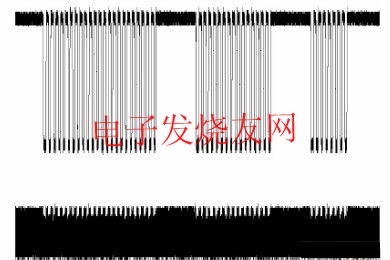
Modulated data and waveform of the antenna
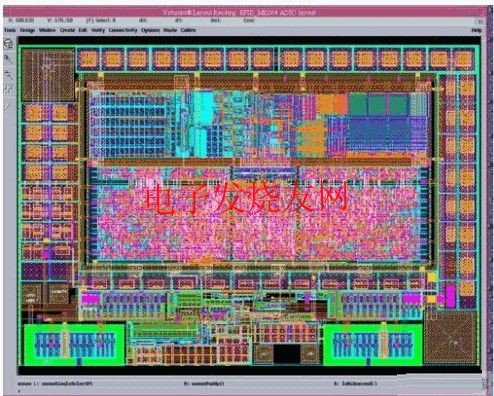
4 ConclusionBased on the SMIC 0.18um one poly four metal standard CMOS process design, the RFID RF front-end circuit conforms to the ISO15693 international standard protocol. The circuit simulation results show that: This RF front-end circuit can effectively recover the DC voltage from the 13.56MHz RF signal. And propose the clock required for the digital part, and demodulate the instruction data. The layout photo of the whole chip is shown in the figure. The area of ​​the chip is 960um*600um. After the film is tested, it can be found to work at 12CM under 7.5A/m field strength. It meets the design specifications.
Rice Mill,Rice Mill Machine,Small Rice Milling Machine,Rice Mill Equipment
Hunan Furui Mechanical and Electrical Equipment Manufacturing Co., Ltd. , http://www.thresher.nl