The CAN (Controller Area NetWork) bus, the Controller Area Network Bus, was originally developed by the German company Bosch in 1982 and is the earliest data communication protocol used between automotive internal measurement and execution components. In more than 20 years of history, CAN bus has been applied in many fields and is the only field bus that has international standards so far. The CAN fieldbus implements the Open System Interconnection (OSI) reference model proposed by the ISO and implements the physical layer, data link layer, and application layer. The CAN controller is used to implement the CAN bus protocol. This text mainly carries on the detailed introduction to the CAN bus communication message acceptance filter, the bit timing and the synchronization, the specific following Xiao Bian together to understand.
First, CAN bus communication packet acceptance filter1, acceptance filter features and functions
1) Characteristics of Acceptance Filters
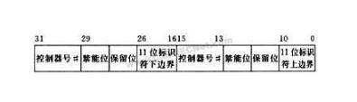
The LPC2000 series ARM microcontrollers are 32-bit embedded microprocessors using the ARM7TDMI-S core with embedded 2- or 4-channel CAN controllers and acceptance filters. The acceptance filter provides global message identification and filtering capabilities for the CAN controller. It contains a 512×32 (2 KB) RAM, and 1 to 5 message identifier tables can be set in the 2 KB RAM to form a lookup table (LUT). The entire lookup table can hold 1024 standard identifiers or 512 extension identifiers, or two mixed types of identifiers. The five possible identifier tables include FullCAN's standard identifier table and independent standard identifier table, standard identifier range table, independent extended identifier table, and extended identifier range table. These five forms do not have to exist at the same time and can be cut as needed. If the start address of a table is equal to the start address of the next table or the value of the table end register, the table is empty and will be ignored in processing.
2) Acceptance filter function
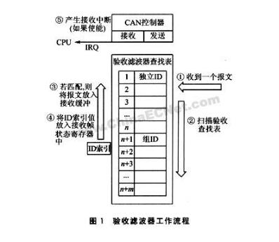
The CAN acceptance filter for LPC2000 series ARM microcontrollers has two operating modes: one is the general mode; the other is called the “FullCAN modeâ€. In normal mode, when the receiving end of the CAN controller receives a complete identifier, it will notify the receiving acceptance filter. The acceptance filter responds to this signal by reading out the CAN controller number and identifier size (standard identifier 11 bits or extended identifier 29 bits); then searching the LUT for a matching identifier. If a matching identifier is found, the CAN controller is notified to place the received message in the CAN controller receive buffer; otherwise, the received frame information is discarded. The workflow is shown in Figure 1.
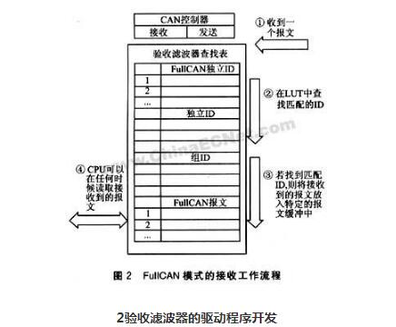
If FullCAN mode is enabled, and the CAN controller reports a standard identifier, the acceptance filter first queries the FullCAN standard identifier table and then processes the reception in FullCAN mode. If no matching ID is found in the FullCAN standard identifier table, the next existing table is sequentially searched until a match is found or the lookup table ends. Once a matching ID is found, the received message is placed into a specific message buffer rather than the CAN controller's receive buffer. This particular buffer is located in the Acceptance Filter's RAM and is in the last part of the LUT. The CPU can read the received message at any time. The reception workflow of FullCAN mode is shown in Figure 2.
2. Acceptance Filter Driver Development
2.1, acceptance filter register description
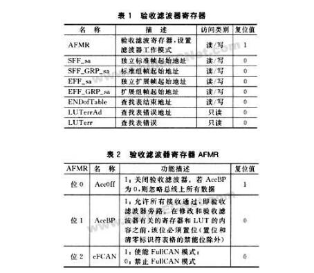
Take LPC2292 as an example to illustrate the development of its acceptance filter driver. In the LPC2292 embedded 2-channel CAN controller, its acceptance filter registers are listed in Table 1. Note: The starting address here is the offset of the base address of the Acceptance Filter RAM. As in the normal mode, SFF_sa=O indicates that the start address of the independent standard frame identifier is located at 0xE0038000.
The size of a table is determined by the difference between the two table start address registers before and after it. For example, SFF_GRP_sa-SFF_sa is the independent standard frame identifier lookup table size. If its value is 0, that is, SFF_GRP_sa=SFF_sa, the size of the independent standard frame identifier lookup table is 0, and this table will be ignored when searching. The look-up table end register ENDofTable represents a lookup table end address, and ENDofTable-EFF_GRP_sa is an extended frame group identifier lookup table size. The acceptance filter register AFMR controls its operating mode. The specific definitions are listed in Table 2.
2.2, lookup table identifier format
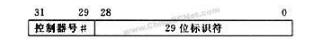
1 FullCAN standard identifier table and independent standard identifier table.
It should be noted that each FullCAN standard identifier table and independent standard identifier table must be arranged in ascending order, ie identifier 1 is greater than the identifier O; otherwise, a table error will be caused in the AF and reception filtering will fail. The table format is as follows:
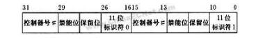
2 standard identifier range table. The ID between the upper and lower borders of the identifier (including the upper and lower borders) is allowed to pass ID. The table format is as follows:
3 Independently expand the identifier table. 1 independent extended identifier takes 1 word and needs to be sorted in ascending order. The table format is as follows:
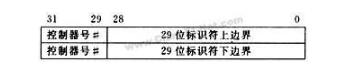
4 Extended identifier range table. It always appears in pairs, occupying 2 words, so legal forms must appear in even numbers and must be sorted in ascending order. The table format is as follows:
2.3, Acceptance filter driver design
According to the above description, the acceptance filter driver can be designed. Take LPC2292 as an example to illustrate how to design a driver.
Assume that there are two independent standard identifiers, ID0 and ID1, which are sorted in ascending order. The range of group standard frame identifiers is ID2 to ID3 (ID2.com.cn - Editor's Note)
3, the conclusion
The CAN acceptance filter of LPC2000 series ARM microcontroller can effectively shield the messages that are not allowed to pass on the bus, which greatly reduces the burden on the CPU. It plays a very important role in the application of the CAN bus for the communication network.
Second, CAN bus bit timing and synchronization explainCAN (Controller Area Network) is a serial communication network that effectively supports distributed real-time control. Considering the synchronization mode of bit timing, it essentially belongs to the asynchronous communication protocol. Each frame is transmitted starting with the start bit of the frame and ending with the end of the frame and the subsequent intermittent field. This requires that the receiver/transmitter must maintain strict synchronization of each bit in the intraframe information code from the beginning of the frame. Considering from the bit timing encoding, it adopts the non-return coding method. Unlike the differential code, the bit stream transmission can directly represent the synchronization signal with the level change. Therefore, in order to guarantee the synchronization quality, the CAN protocol defines its own bit synchronization method. : Hard synchronization and resynchronization.
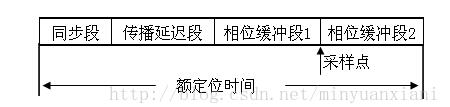
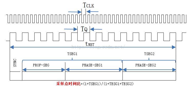
1, the structure of the bit cycle
2, synchronization mechanism
Bit synchronization on the CAN bus is only generated when the node detects a transition from a "recessive bit" (logical 1) to a "dominant bit" (logical 0), when the transition edge is not within the synchronization period of the bit period. Phase error will occur. The phase error is the distance between the jumping edge and the end of the sync segment. If the transition edge occurs before the synchronization section, the phase error is positive before the sampling point; if the transition edge is located before the synchronization section, the sampling phase is negative phase error. The phase error results from oscillator drift of the node, propagation delay between network nodes, and noise interference. The CAN protocol specifies two types of synchronization: hard synchronization and resynchronization.
2.1, hard synchronization
Hard synchronization is accomplished only with a falling edge (start of frame) when the bus is idle, and the bit times of all nodes restart with or without a phase error. The edge of the transition that forces the hard synchronization to occur is within the sync segment of the restarted bit time.
2.2, resynchronization
In subsequent bits of the message frame, whenever there is a transition from a "recessive bit" to a "dominant bit", and the transition falls outside the synchronization segment, a resynchronization will result. The resynchronization mechanism can increase or decrease the bit time according to edge transitions to adjust the sampling point position to ensure correct sampling.
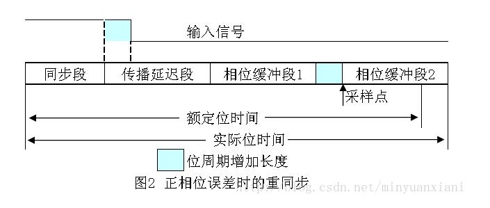
As shown in Figure 2, the edge of the transition falls before the sample point after the sync segment. It is a positive phase error and the receiver considers this to be a slow-transmitter-delayed edge. At this point, the node will grow its own phase buffer segment 1 (shaded) in order to match the sender's time. The increase time is the absolute value of the phase difference, but the upper limit is the resynchronization jump width SJW.
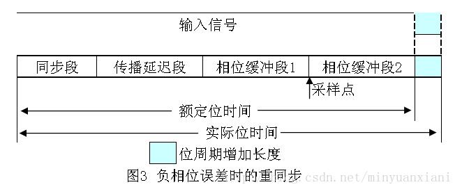
As shown in Figure 3, the transition edge falls before the sync segment after the sample point, which is a negative phase error. The receiver interprets it as an advance edge of the next bit period sent by a fast transmitter. The same node will shorten its own phase buffer segment 2 (hatched portion) in order to match the time of the transmitter, and the next bit time will start immediately. The shortened time is also the absolute value of the phase difference, and the upper limit is the resynchronization jump width SJW.
The phase buffer segment is only incremented or shortened during the current bit period. The next bit period, as long as there is no resynchronization, will return to the programmed preset value for the bit time.
When the absolute value of the phase difference is less than or equal to the resynchronization jump width SJW, the effects of resynchronization and hard synchronization are the same, and the phase difference compensation can be realized; but if the absolute value of the phase difference is proportional to the synchronization jump width, due to The maximum compensation value is the resynchronization jump width, so that the resynchronization cannot completely compensate for the phase difference.
The bit filling mechanism of CAN protocol not only realizes the transparency of data of arbitration field, control field, data field and CRC sequence, but also increases the chance of jumping from “recessive bit†to “dominant bitâ€, that is, increase the weight. The number of synchronizations improves synchronization quality. The bit-stuffing principle guarantees that there will be no more than 10 bit periods (ie, 5 dominant bits, 5 recessive bits) between the resynchronization jump edges without any error, and the actual system will Errors occur, so that the interval between the actual two resynchronization jump edges may be 17 to 23 bit times (active error flags and their superposition 6 to 12 bit times, error delimiters 8 bit times, intermittent fields 3 bit time).
3, the conclusion
In the actual system design, the user can optimize the bit timing parameters of the CAN controller according to factors such as the oscillator clock frequency, bus baud rate, and the maximum transmission distance of the bus, and coordinate the two main factors affecting the timing setting of the bit. : Oscillator tolerance and maximum bus length. Reasonably arrange sampling point positions and sampling times in the bit cycle to ensure effective synchronization of the bit stream on the bus. At the same time optimize the communication performance of the system and further promote the wide application of CAN bus.
Calcium fluoride is often used in spectroscopic windows and lenses due to its high transmission from 200nm to 7μm. Its low absorption and high damage threshold makes it a popular choice for excimer laser optics. Calcium fluoride's low index of refraction allows it to be used without an anti-reflective coating. The Knoop hardness of calcium fluoride is 158.3. Calcium Fluoride (CaF2) Windows manufactured from vacuum UV grade calcium fluoride are commonly found in cryogenically cooled thermal imaging systems.
Caf2 Windows and Lens,Ir Caf2 Windows,Ir Caf2 Lens Single,Crystal Caf2 Windows
Zoolied Inc. , https://www.zoolied.com