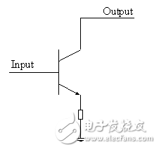
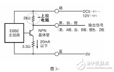
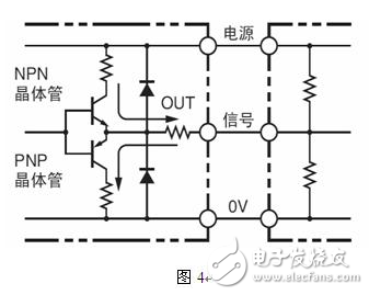
The **first concept is the open collector output**. This principle is illustrated in the diagram below. When the transistor is activated, the collector output goes low. However, when the transistor is turned off, the collector remains in a high-impedance state, also known as "floating." Because of this, an external pull-up resistor and a power supply are necessary for the circuit to function properly. By selecting the appropriate resistance value and power supply voltage, it is possible to ensure that both the high and low output levels meet the required specifications. Additionally, this setup helps prevent excessive current from flowing through the output transistor, making it ideal for interfacing with various devices.
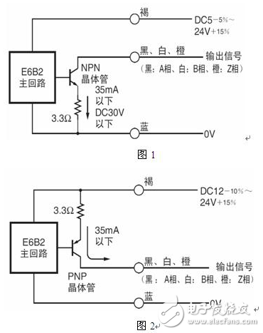
**Second, there are two types of open collector outputs**: NPN and PNP. An open collector output typically uses the emitter as a common terminal, while the collector is left open. These configurations are commonly used in digital circuits to allow multiple devices to share a single line or to interface with different types of logic families.
In an **NPN open collector output**, the transistor is made up of three layers: two N-type semiconductors with a P-type layer in between. The NPN transistor allows current to flow from the collector to the emitter when the base is forward-biased. In normal amplification mode, the collector voltage is higher than the base, which is higher than the emitter. This makes it suitable for applications where a low-level signal needs to be pulled up using an external resistor.
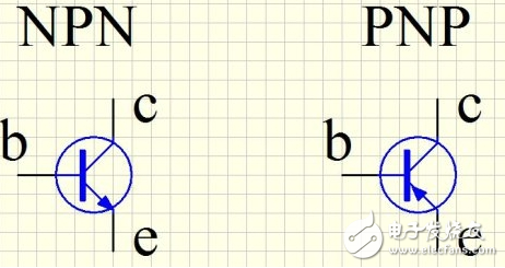
On the other hand, a **PNP open collector output** consists of two P-type layers with an N-type layer in the middle. Here, current flows from the emitter to the collector when the base is forward-biased. In normal operation, the emitter has the highest voltage, followed by the base, and then the collector. This configuration is often used in circuits where a high-level signal needs to be pulled down.
**Third, let's compare different output types: voltage output, complementary output, and linear drive output**.
1. **Voltage Output** – This type is based on the open-collector circuit. A pull-up resistor is connected between the power supply and the collector, allowing the output to reach a stable high voltage level. This method is simple and effective for basic digital applications.
2. **Complementary Output** – This circuit uses both NPN and PNP transistors on the output side. Depending on whether the output signal is high or low, the corresponding transistor turns on or off. This configuration offers better performance compared to a simple open collector output and can be used with both NPN and PNP input devices.
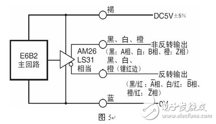
3. **Linear Drive Output** – This type uses differential signaling, such as the RS-422 standard, and is commonly implemented with chips like the AM26LS31. It provides strong noise immunity and is ideal for long-distance and high-speed data transmission. However, it requires a receiver capable of interpreting differential signals.
Each of these output types has its own advantages and is suited for different applications, depending on the requirements of the system. Understanding their differences helps in choosing the right one for your design.
Solar Panel,,High Efficiency Mono Solar Panels,Bifacial Jinko Solar Panels
PLIER(Suzhou) Photovoltaic Technology Co., Ltd. , https://www.pliersolar.com