In recent years, Field Programmable Gate Arrays (FPGAs) have gained widespread adoption due to their high performance, cost-effectiveness, rapid development cycle, and ease of programming. However, the rise of Differential Power Analysis (DPA) attacks on FPGAs has become a significant threat to information security in FPGA-based applications, drawing considerable attention from researchers and developers.
DPA is a type of Side Channel Attack (SCA) that exploits the relationship between power consumption and internal cryptographic keys. By analyzing power consumption patterns during cryptographic operations, attackers can infer secret keys by correlating power traces with guessed key values. The core idea involves dividing the power waveform data into two groups based on a guessed key, and then comparing the power consumption differences between these groups. If the guess is correct, the resulting differential curve will show distinct peaks, making it easier for an attacker to identify the correct key.
The fundamental cause of DPA vulnerabilities lies in the asymmetry of the circuit's logic representation. To address this, this paper explores the application of FPGA’s inherent structural features combined with established circuit-level countermeasures against DPA attacks. A deep analysis of these protection techniques on the FPGA platform is conducted to enhance security and resilience against side-channel threats.
**1 Circuit Protection Technology on FPGA**
**1.1 The Underlying Structure of FPGA**
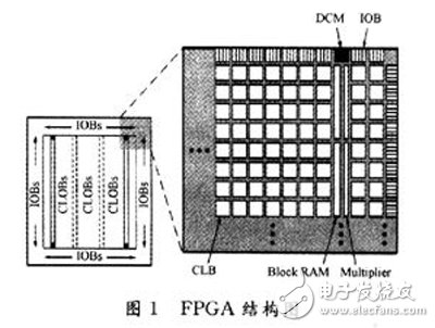
The simplified architecture of an FPGA is illustrated in Figure 1. Key components include the Configurable Logic Block (CLB), Input/Output Block (IOB), Block RAM, Digital Clock Manager (DCM), and Multiplier. Among these, the CLB is the primary unit responsible for implementing programmable logic. For example, a slice in the Virtex-5 FPGA contains four 6-input lookup tables, four flip-flops, and several multiplexers, enabling complex logic functions.
**1.2 Implementation of Dual-Track Circuit Technology**
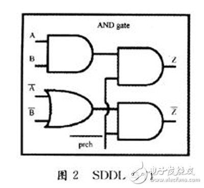
Dual-track circuit technology represents both input and output signals using two lines. As shown in Figure 2, an SDDL AND gate uses two lines to represent signal A and output Z. This allows a variable to have four possible states: (0,0), (0,1), (1,0), and (1,1). In SDDL, (0,1) and (1,0) are used to represent logic 0 and 1, respectively, ensuring symmetry in power consumption. Additionally, a precharge signal (prch) is introduced, which sets the output to (O,0) during the precharge phase. The circuit operates in two modes: precharge and operational. These modes alternate, controlled by a fixed-period pulse on prch. This ensures that only one signal line changes at a time, balancing power consumption and reducing leakage.
**1.3 Implementation of Pre-Charge Technology**
Standard logic gates do not support continuous activity, leading to independent data states. To address this, a precharge circuit is added. When the clock is high, the precharge phase begins, setting the output to logic 0. When the clock is low, the calculation phase starts, completing the actual computation. Using precharge logic in FPGAs ensures that the output of each slice is logic 0 during the precharge phase.
There are two main approaches to implement precharge functionality:
1. **Clocked Multiplexer:** A clocked multiplexer is used to implement the precharge function, with a dedicated register in each slice. However, this method requires generating complementary clock signals, increasing power consumption and complexity.
2. **Asynchronous Clear Latch:** Using a memory unit as an asynchronous clear latch with a reverse enable input provides a simpler solution. It requires only a single signal, but may necessitate a special register within the slice.
**2 DES Encryption Module Implementation**
To protect critical components and ensure constant power consumption, a security shield is implemented on the FPGA. Here, we use dual-rail and precharge technologies to create a secure design. Modern FPGA implementations require precise control over placement and routing to achieve optimal performance.
The implementation of the DES encryption module includes the hardware macro for the S-box and the core encryption logic. The S-box is a crucial part of the DES algorithm, and its design significantly impacts overall performance. In FPGA implementation, it is essential to leverage the device's configurable resources efficiently while considering internal structure for optimal results.
Due to the limitations of integrated tools, the output netlist is often difficult to interpret. To overcome this, a hardware macro, or hard macro, is created. This approach takes full advantage of the FPGA Editor’s capabilities to implement dual-rail and precharge techniques directly from the infrastructure configuration, offering greater control and efficiency.
Indoor Rental Stage Events Led Wall
Indoor rental stage events LED walls are large LED video walls that are used for indoor events such as concerts conferences, trade shows, and exhibitions. These LED walls are made up of multiple LED panels that can be easily assembled and disassembled for rental purposes.
Indoor Rental Stage Events Led Wall,Stage Events Led Display Panels,Music Concerts Stage Led Screen,Indoor Stage Rental
Guangzhou Cheng Wen Photoelectric Technology Co., Ltd. , https://www.cwledwall.com