In recent years, Field Programmable Gate Arrays (FPGAs) have gained widespread adoption due to their high performance, cost-effectiveness, rapid development cycle, and ease of programming. However, the emergence of Differential Power Analysis (DPA) attacks on FPGAs has become a significant threat to the security of information systems utilizing these devices, prompting considerable research and attention in the field.
DPA is a type of Side Channel Attack (SCA), which exploits the relationship between power consumption and the internal cryptographic key. By analyzing power waveform data during cryptographic operations, attackers can infer the secret key by dividing the data based on guessed keys. When the correct key is used, the resulting power difference curve will exhibit distinct spikes, revealing the internal state of the circuit.
The root cause of DPA vulnerabilities lies in the asymmetry of the circuit’s logic representation. This paper explores how FPGA's inherent structural characteristics can be leveraged alongside traditional circuit-level countermeasures against DPA attacks. A detailed investigation into these protection techniques on an FPGA platform is conducted to enhance the security of cryptographic implementations.
**1 Circuit Protection Technology on FPGA**
**1.1 The Underlying Structure of FPGA**
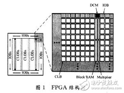
The basic structure of an FPGA is illustrated in Figure 1. Key components include the Configurable Logic Block (CLB), Input/Output Block (IOB), Block RAM, Digital Clock Manager (DCM), and Multiplier. Among these, the CLB serves as the primary unit for implementing programmable logic. In a Virtex-5 slice, each contains four 6-input lookup tables, four flip-flops, and several multiplexers.
**1.2 Implementation of Dual-Track Circuit Technology**
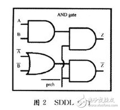
Dual-track circuit technology represents both inputs and outputs using two signal lines. For example, in an SDDL AND gate, signal A is represented by A and its complement, while the output Z is also represented by Z and its complement. This allows for four possible logical states: (0,0), (0,1), (1,0), and (1,1). SDDL uses (0,1) and (1,0) to represent logic 0 and logic 1, respectively, making the internal logic symmetric and ensuring equal power consumption for both values.
Additionally, a precharge signal (prch) is introduced. During the precharge phase, the output is set to (0,0), representing a neutral state. The circuit operates in two modes: precharge and operational. These phases alternate, with prch controlled by a fixed-frequency pulse. As a result, only one signal line changes at a time, achieving balanced power consumption across all logic states.
**1.3 Implementation of Pre-Charging Technology**
Standard logic gates do not provide continuous activity, leading to unpredictable power consumption patterns. To address this, a precharge circuit is added. When the clock is high, the precharge phase begins, setting the output to logic 0. When the clock is low, the calculation phase starts, completing the actual computation.
On an FPGA, precharge logic ensures that the slice output is always logic 0 during the precharge phase. Two approaches are commonly used:
1. **Clocked Multiplexer**: A separate memory unit is used as a register, but it operates on a reverse clock. This method increases power consumption and complicates routing due to the need for clock signal duplication.
2. **Asynchronous Clear Latch**: A memory unit is configured as a latch with a reverse enable input. This approach simplifies the design by using a single signal for both registers and latches, though it requires specialized hardware.
**2 DES Encryption Module Implementation**
To protect critical components from DPA attacks, a security shield is implemented on the FPGA to maintain constant power consumption. This project employs dual-rail and precharge logic to achieve this goal. Modern FPGA design demands precise control over placement and routing.
The implementation of the DES encryption module involves two main aspects: the S-box hardware macro and the core encryption logic. The S-box is a crucial component of the DES algorithm, and its design significantly impacts overall performance. In FPGA implementation, resource efficiency and speed are prioritized, requiring careful consideration of the device’s internal architecture.
Due to the complexity of integrated tools, designers often struggle to understand the final netlist. To overcome this, a hardware macro, or hard macro, is created. This approach leverages the FPGA Editor’s capabilities to implement dual-rail and precharge techniques directly from the infrastructure configuration, offering greater control and optimization.
Stage Led Strobe Light ,Nine Eyes Laser Strobe Light,Stage Strobe Lights,Stage Led Strobe Lights
Guangzhou Cheng Wen Photoelectric Technology Co., Ltd. , https://www.cwledwall.com