Abstract : With the increase of the complexity of aviation system integration, how to effectively monitor bus data behavior, real-time data analysis, fault diagnosis and location is an important issue for avionics systems. A design scheme of ARINC659 bus analyzer based on FPGA is proposed, which mainly realizes monitoring, sampling, storage and fault injection test of ARINC659 bus data. It can trigger bus data real-time analysis and evaluate bus behavior through communication interface, which is ARINC659 bus data. Real-time analysis provides a complete and reliable test.

The development of avionics system integration is constantly improving, and the requirements for system security, fault tolerance and real-time are getting higher and higher. The backplane bus is an integral part of the data transfer between the online replaceable modules (LRMs) in the avionics system. The increased complexity of aviation system integration makes it an important issue for avionics systems to efficiently monitor bus data behavior, analyze data in real time, and perform fault diagnosis and location. Providing a system that can trigger transient monitoring to analyze the communication status between LRMs will greatly improve the maintenance efficiency of avionics systems and reduce the maintenance time of system faults, which will play a significant role in improving the maintainability and availability of equipment [1].
This paper proposes an ARINC659 bus analyzer system design based on FPGA, which can complete the ARINC659 bus data monitoring, fault injection, simulation test and other functions.
1 program design1.1 Transmission mechanism
ARINC659 is a serial bus that uses four serial buses to communicate through half-duplex communication and cross-checking. It reduces hardware circuits and improves reliability. ARINC659 is a dual-bus configuration of dual bus. The bus pairs A and B respectively have two buses of “x†and “yâ€. Each bus has one clock line and two data lines, each transmitting 2 data bits, complete. The bus consists of 12 lines.
ARINC659 adopts dual bus cross-detection fault-tolerant mechanism. The received data is first decoded accordingly, and the data is cross-correlated according to the received data validity and the decoded four bus data (AX=AY, BX=BY, AX=BY, AY= BX) comparison, the comparison results determine the validity of the data according to the call availability table or the integrity table.
The command table mainly completes bus initialization and pre-decoding commands, and performs communication between nodes in the system and configuration of each task of the node.
1.2 Working principle
The bus analyzer is attached to the ARINC659 bus like other LRM modules. Figure 1 shows the bus analyzer in the system. The bus analyzer has the same bus command table as the other LRMs in the system. If the bus analyzer is Set to the analysis mode, when the system power-on bus starts data communication, when any LRM sends data to the bus, the bus analyzer starts to receive all the data on the bus, analyzes and processes the data message and the synchronization message, and monitors through the host. The interface displays the status of the bus data in real time. The bus analyzer only receives the data on the bus and does not send or change the data on the bus. The ARINC659 bus specifies that only one transmitter can be used in one window, or the backup transmitter can send data to the bus. Allows multiple devices to receive bus data, and configures the command table to configure the bus analyzer only as a receive state. The bus analyzer receives the bus data through the bus transceiver and samples the bus data with a clock frequency of 240 MHz. The acquisition module performs front-end processing on the data, transmits it to the processor for bus protocol analysis and data analysis, and transmits the bus state through the Ethernet. To the application layer software, the application layer displays the bus state information in real time through the GUI interface after the data is processed. When the bus analyzer is used as the fault injection mode, the bus analyzer acts as an input device to set the open circuit fault of the bus data or to lower the fault setting. The bus injection error causes a bus error [2].
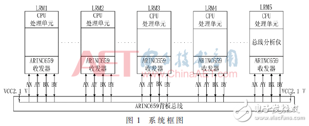
The bus analyzer power-on initialization completely follows the ARINC659 bus power-on initialization and synchronization specification. After the power-on initialization is completed, it is in the monitoring bus state, and the data on the bus is transmitted to the host in real time to complete the analysis and display of the bus data.
1.3 Hardware Design
The ARINC659 bus analyzer is mainly composed of a power supply circuit, a reset circuit, a bus transceiver circuit, a bus relay circuit, a data acquisition unit (FPGA and configuration circuit), and a CPU data processing unit. As shown in the functional block diagram of Figure 2, the data acquisition unit performs high frequency data sampling of the bus data; the CPU data processing unit is responsible for processing the bus data and real-time transmitting the bus status to the host. The CPU data processing unit requires a CPU module with a certain memory, and has a PCI interface and an Ethernet.
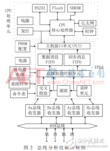
The power circuit is the power supply module of the entire system, providing the working voltage required for the operation of each chip of the entire system.
The reset circuit implements a system reset mechanism using three reset modes: manual reset, power-on reset, and soft reset.
Suizhou simi intelligent technology development co., LTD , https://www.msmvape.com