MOS transistors often need to be biased in the weak inversion region and the mid-inversion region, which is to obtain higher gain at the same bias current in the future. At present, the popular MOS tube models can be roughly divided into two categories. This paper will explain the types of MOS tube models and the model diagrams of NMOS.
When it comes to the model of MOS tube, everyone should be familiar. For different applications and needs, we have to choose the appropriate model. For example, in digital circuits, a simple switching model or a resistor-capacitor (RC) model is typically used. In analog circuits, models suitable for different bias conditions and different frequencies are required. For submicron devices, short channel effects such as channel length modulation and speed saturation are also considered. The BSIM (Berkeley Short-channel IGFET Model) model, invented by the research team at the University of California, Berkeley, was used in the simulation software. In IC design, the first step is often hand calculaTIon, and the BSIM model has hundreds of parameters, so we often use a simplified model when we calculate it again. The most familiar one is the square rate model. However, the square-rate model has two major limitations. One is that it is difficult to include many short-channel effects, and the other is only applicable when the MOS tube is biased in a strong inversion. In many circuits, in order to achieve higher gain at the same bias current, or to reduce power consumption at the same gain, MOS transistors often need to be biased in the weak inversion region and the mid-inversion region. Therefore, we need a continuous inversion, moderate inversion, and weak inversion to be continuous and accurate, and can contain a variety of short channel effects. The model of the calculation.
The current popular MOS tube models can be roughly divided into two categories. One is based on a threshold voltage-based model. Typical representatives are BSIM3 and BSIM4. You can refer to Razavi's textbook. A typical feature of this is that the threshold voltage is a function of Vsb to characterize the body effect. This type of model has greater limitations in deep submicron processes. Another type of charge-based model is represented by the BSIM6 and EKV models. The BSIM6 model is the standard model for CMOS processes in today's simulation tools (released in 2013). The EKV model taught by Professor Abidi in the classroom can provide a lot of design guidance in the hand calculation process. (EKV, named after the names of its three inventors Enz, Krummenacher, Vittoz).
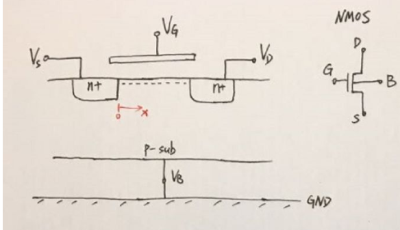
As shown in the figure below is an NMOS model diagram. The MOS transistor is a four-terminal device including a source terminal (S), a drain terminal (D), a gate terminal (G), and a substrate (B). In a standard CMOS process, all MOS transistors share a P-type substrate. To prevent the PN junction from being forward biased, the P-type substrate is typically connected to GND. Vs, VD, VG are all defined relative to the substrate voltage. The source and drain are completely symmetrical, gradually increasing the gate voltage, and an inversion layer appears on the surface of the device. For the NMOS, the inversion layer is composed of electrons. The inversion layer is very thin and its thickness can be neglected (Charge-Sheet ApproximaTIon), so we use a simple one-dimensional model in the analysis. In the figure, the source is extremely origin, and the source is led to the drain to draw the x-axis.
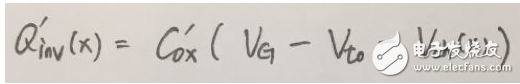
As shown in the figure below, we will record the surface charge density of the inversion layer at coordinates x as Qinv'(x), where the channel voltage (relative to the substrate) is denoted as Vch(x),
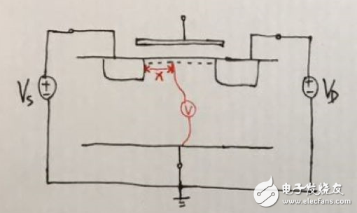
The gate, the inversion layer and the sandwiched oxide layer in the middle can be seen as a parallel plate capacitor. The relationship between the charge density of the inversion layer and the voltage between the two plates is as follows:
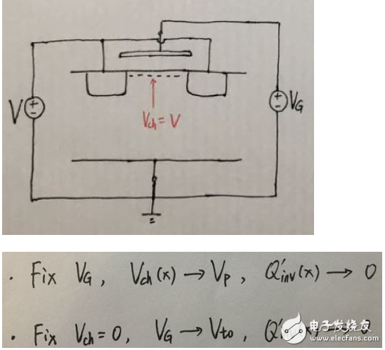
Below we define two important concepts: the pinch-off voltage (Vp, pinch-off voltage) and the threshold voltage (Vt0, threshold voltage). In the figure below, the source and drain remain at the same potential, so that the potential of the entire channel is the same. If VG is fixed, the inversion layer charge density is reduced to 0 when the channel voltage is increased to Vp; if the fixed channel voltage is 0 V, the inversion layer charge density is reduced to 0 when VG is reduced to Vt0. Here, the threshold voltage Vt0 is defined under the condition that the entire channel is equipotential and the potential is zero, and thus is a constant value. In contrast, the threshold voltage VTH in the conventional model is a function of Vsb. It is also worth noting that the definition of the pinch-off voltage Vp is effective only when the source drain is equipotential, as long as the voltage Vch(x) at a certain point in the channel is greater than Vp, at which point the channel is pinched off.
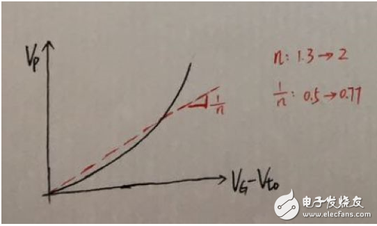
The relationship between the pinch-off voltage and the gate voltage is shown in the figure below. This nonlinearity is caused by the nonlinearity of the barrier capacitance Cdep below the inversion layer (we will elaborate in the introduction of the MOS tube capacitance model). To simplify the model, it is usually approximated by a straight line with a slope of 1/n, ie Vp = (VG-Vt0)/n. In the subsequent calculations we use n = 1.5. Note: Sometimes the nonlinear relationship between Vp and VG-Vt0 will cause the large signal bias circuit to be inoperable. Specifically, we will introduce that n is greater than 1 and less than 1, indicating that the simultaneous inequality has no solution. In this example, we will give an example when we introduce the bias circuit later.
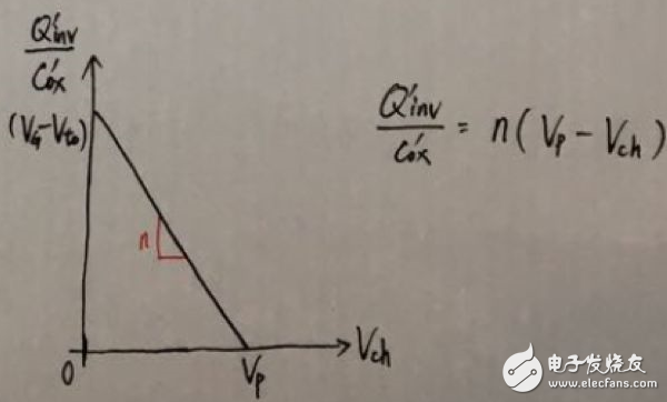
Based on the above approximation, the relationship between Qinv' and Vch can be drawn. When Vch = Vp, the channel is pinched off and the charge density is 0; when Vch = 0, Qinv' = Cox'*(VG – Vt0). Careful children's shoes may have noticed that the relationship in the figure below is slightly different from the formula for the parallel-parallel capacitors listed above, because the previous formula is to ignore the effect of the barrier capacitance Cdep, or at n = 1. Launched under conditions.
â–¶ The Cigfun 2000 puffs disposable e-cigarette has a 6ml oil capacity, 850mAh battery. It is an easy to carry, portable e-cig. Adopt mesh coil vaporizer, it is powerful and maximum flavor, bring natural, purest taste.
â–¶ Cigfun disposable vape pen is produced in ISO9001, GMP workshop, thus the quality can be guaranteed, safe and healthy than refillable vape pod.
â–¶ Disposable e-cigarettes are compact, lightweight and easy to carry, the auto draw system, no button needed, just open the package, near to your mouth, then smoke.
â–¶ Cigfun disposable vape bar has nic salt 2%, 3%, 4%, 5%, meet your every need. Amazing flavors include kiwi ice, apple ice, gummy bear, green apple, bubble gum, cool mint, Strawberry ice Cream, Peach Ice, Coconut melon, Energy Strawberry, Sour Apple, Kiwi guava, Watermelon Mango Peach, Banana Milk.
â–¶ Axiswell is the world's leading manufacturer of Vape Pens. Our business covers ENDS (Electronic Nicotine Delivery Systems) and other vaping devices, such as disposable vape, refillable vape pen, pod system, CBD vape pen, cbd pods, etc. We maintain factory price, good quality, providing vapers safe and competitive price vaping products.
Moreover, we're dedicated to establishing a healthy and sustainable environment for the whole vaping industry.
Cigfun Vapes Disposable,Disposable Vape Pod,Cigfun 1500 Puffs,Cigfun 2000 Puffs Vape,Cigfun 2500 Puffs Vape Pod
Shenzhen Axiswell Technology Co., Ltd , https://www.medhealthycare.com