As an important development in embedded computing design using FPGAs and high-speed I/O, the latest mezzanine card standard called FMC+ will extend the total number of Gigabit Transceivers (GTs) in the card from 10 to 32, the largest The data rate has been increased from 10Gbps to 28Gbps while maintaining backward compatibility with current FMC standards.
These features also fit well with new devices using the JESD204B serial interface standard, as well as 10G and 40G optics and high-speed serial memories. FMC+ meets the most challenging I/O requirements, giving developers a double benefit: the flexibility of mezzanine cards and the high I/O density of single-chip designs.
The FMC+ specification was developed and refined last year. The VITA 57.4 working group has approved the specification and will submit an ANSI vote in early 2016. Let's take a closer look at this important new standard and understand its impact on advanced embedded design.
Advantages of mezzanine cards
Mezzanine cards are an effective and widely used method of adding specific functionality to embedded systems. Because the mezzanine card is attached to the base card or carrier card, not directly
1st Quarter 2016 Xilinx China Newsletter Page 53
The mezzanine card can be easily replaced on the back panel. For system designers, this means both flexible configuration and easy upgrades. However, due to connectivity issues or the extra space required to install on the development board, this flexibility often comes at the expense of functionality.
For FPGAs, the main open standard is ANSI/VITA 57.1, also known as the FPGA Mezzanine Card (FMC) specification. The latest standard, FMC+ (more formally, VITA 57.4) extends the capabilities of the existing FMC standard by significantly enhancing the functionality of the Gigabit serial interface.
Compared to single-chip solutions, FMC+ addresses many of the deficiencies of mezzanine-based I/O while providing greater flexibility and performance. At the same time, the FMC+ standard is backward compatible, in line with the development history of FMC and meet the needs of its user community.
The FMC standard defines a small mezzanine card that is similar in height and width to a mature MMC or PMC, but only half the length. This means that FMC has a smaller board-level space than the open standard format. However, FMC does not require a bus interface that often takes up a lot of board space, such as PCI-X. Instead, the FMC communicates with the master FPGA using a direct-connect I/O with a relatively simple power supply requirement. This means that although the size is smaller, the FMC actually
Like the XMC equivalent of their larger I/O capacity and the PMC and XMC specifications, both FMC and FMC+ offer both air cooling and conduction cooling, so both commercial and military markets demand common and durable applications. Can be applied.
The FMC specification is fairly straightforward to parse. The standard provides up to 160 single-ended or 80 differential parallel I/O signals for high pin count (HPC) designs, providing half the number of I/O signals for low pin count (LPC) designs. Up to 10 full-duplex GT connections can be set. These GTs are suitable for fiber optics or other serial interfaces. In addition, the FMC specification defines key clock signals. All of these I/Os are optional, although most hosts now support full connectivity.
The FMC specification also defines a variety of power inputs, although the mezzanine card defines the power supply from the host. This method works by first powering the mezzanine card section so that the host can interrogate the FMC and then the FMC responds by defining a voltage range for the VADJ. If the host is able to provide this voltage range, everything goes smoothly. Not setting the main power adjustment on the mezzanine card can save space and reduce the power consumption of the mezzanine card.
FMC for analog I/O
Designers can use FMC as a feature for any user who wants to connect to an FPGA, such as digital I/O, fiber optics,
Control interface, memory or additional processing. However, analog I/O is still the most common use of FMC technology. The FMC specification applies to a wide range of fast, high-precision I/O, but it also needs to be weighed, especially for high-speed components that use parallel interfaces.
For example, Texas Instruments' ADC12D2000RF dual 2 Gsps 12-bit ADC uses a 1:4 multiplexed bus interface, so this bus speed is not too fast for the master FPGA. The digital data interface requires 96 signals alone (48 LVDS pairs). For this class of devices, the FMC can only support one such device, and the FMC has an upper limit of 160 signals, even if there is enough room for more devices. Even lower precision devices operate at higher speeds, such as those operating on 8-bit data channels, allowing for more channel counts even with higher front-end analog coupling requirements for converters, amplifiers, clocks, and more.
For analog interfaces that use a parallel interface running at 5 Gsps or 6 Gsps (throughput greater than 50 Gbps) with accuracy greater than 8 bits, the FMC specification cannot begin to cope. From a market perspective, mainstream FMC throughput is between 25-50 Gbps in terms of channel density, speed and accuracy. This level of performance is the result of the physical package size and the available connections to the master FPGA.
In addition to parallel connections, the FMC specification supports up to 10 duplex high speed serial (GT) links.
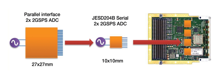
Figure 1 - FMC reduces the impact of packaging with JESD204B 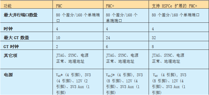
Figure 1 - FMC uses JESD204B to reduce the impact of packaging.
These interfaces are useful for emerging technologies such as fiber I/O, Ethernet, Hybrid Memory Cube (HMC) and Bandwidth Engine, and next-generation analog I/O devices that use the JESD204B interface.
JESD204B coming
Although the JESD204 serial interface standard (currently revision "B") has been around for a while, it has only recently been widely adopted by the market as a serial interface standard for a new generation of high sample rate data converters. The driving force behind this widespread adoption comes from the telecommunications industry's desire for smaller, lower power and lower cost devices.
As mentioned earlier, dual-channel 2 Gsps, 12-bit ADCs with parallel interfaces require a large number of I/O signals. This requirement directly affects the package size. In this case, a 292-pin package is required, which is approximately 27x27mm (although the next-generation pin geometry can shrink package size to less than 20x20mm).
The equivalent device with JESD204B connection can be packaged in a 68-pin, 10x10mm package with lower power consumption.
This shrinking package size is well matched to evolving FPGAs as FPGAs are providing an ever-increasing number of GT links that are growing in speed. Figure 1 shows an example of the package size and the FMC/FMC+ development board size.
Depending on the data throughput, accuracy, and number of analog I/O channels required for the sample rate, a typical high speed ADC and DAC using the JESD204B interface has 1-8 GT links operating at 3-12 Gbps.
The FMC specification defines a relatively small-sized mezzanine card, but with the rise of the JESD204B device, more components can be accommodated in the board-level space. Up to 10 GT links defined by the FMC specification are one available. It is this limited number of GT links that can provide 80 Gbps or higher throughput by using only a fraction of the number of pins required for parallel I/O.
The rise of serial-connected I/O devices using interfaces such as JESD204B has indeed brought deficiencies to some of the subdivision applications of electronic warfare, such as digital radio frequency memory (DRFM). Due to the long data pipeline, serial interfaces inevitably bring greater
Delay. For DRFM applications, the delay between data input and data output is a fundamental performance parameter. While the delays between serial connected devices tend to be very different, next-generation devices will allow data to pass through the pipeline at a faster and faster rate, some of which are expected to have the ability to adjust the pipeline depth. It remains to be seen how much improvement can be achieved.
Today's standard ADC devices with partial sampling rates greater than 1 Gbps have latency less than 100 ns. Other applications can tolerate this delay, or ignore it, including software-defined radio frequency (SDR), radar warning receivers, and other signal intelligence (SIGINT) subdivisions. Driven by mass-market telecommunications infrastructure, the new generation of RF ADCs and DAC technology is widely used, and these applications have gained significant advantages.
Beyond the FPGA community, next-generation DSP devices are also starting to adopt JESD204B. However, it is very likely that the FPGA will still be able to take up the position that best utilizes the capabilities of the wideband analog I/O devices. This is because FPGAs can handle huge amounts of data with better parallelism.
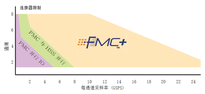
Figure 2 - Comparison of throughput energy between FMC and FMC+ digitizer
Evolution of FMC+
To take the FMC to a whole new level, the VITA 57.4 working group has developed a specification using a larger number of GT links operating at higher speeds. FMC+ simply adds an outer column to the FMC connector to handle more signals, without changing any board shape or mechanical structure, so it has full FMC backward compatibility.
New rows can form part of an enhanced connector, minimizing the footprint of available board space. The FMC+ specification increases the maximum number of available GT links from 10 to 24 and optionally adds another 8 links to achieve a total of 32 full-duplex links. The extra link uses the HSPCe separate connector (HSPC primary connector). Table 1 is an overview of FMC and FMC+ connections
Multiple independent signal integrity teams characterized and validated higher 28Gbps data rates. With parallel interfaces, the maximum duplex throughput in each direction can now exceed 900 Gpbs. See Figure 2 for a sketch of the net throughput that is expected to be achieved for a digital solution that supports both FMC and FMC+.
Designers can take advantage of the new throughput of FMC+ to take advantage of new devices that offer massive I/O bandwidth. There is still a trade-off here, such as how many devices can fit into the usable space of the mezzanine card, but for a modest number of channels, the achievable throughput is a huge leap compared to today's FMC specification.
Next generation ADC and DAC
In the next few years, it is reasonable to expect that high-precision ADCs and DACs will break through 10 Gsps barriers, using direct RF sampling to support extremely wide-bandwidth communications at L-, S-, and even C-band frequencies. Below 10 Gbps, 12-bit, 14-bit, or even 16-bit precision converters are emerging, with some supporting multiple channels. Most of these devices will use JESD204B (or newer) signal processing with 12 Gbps channels until a new generation of products takes this speed to new heights. The driving force behind these rapid developments comes from the telecommunications industry, but the defense industry can also take advantage of size, weight and cost (SWAP-C) requirements.
Advantages and uses of other FMC+
Although similar to FMC, FMC+ is also likely to be dominated by ADCs, DACs, and transceiver products, and the larger GT density offered by FPGAs allows it to be used for other functions. Two features worth mentioning are fiber optics and new serial memories.
As with JESD204B, there is a need for faster, denser fibers. Devices that use fiber optic strips minimize component size. Because the FMC+ space immediately supports 24 full-duplex fiber links, and with the higher speeds supported by FMC+, the application is likely to be the first to implement. The 28Gbps bandwidth of each fiber will allow throughput to quickly move through the 100G and 400G barriers of single-chip mezzanine cards. The 100G optical transmission capability on the current FMC format is emerging today.
Another emerging area for FMC+ is serial memory such as Hybrid Storage Cube (HMC) and MoSys' Bandwidth Engine. These novel devices are a new class of high-performance memory that delivers unprecedented system performance and bandwidth with GT connectivity. (Xilings China Newsletter No. 43, check out these new memory types.)
呱呱 landing
A new generation of FMC specifications has been introduced that are adapting to new technologies driven by serial-connected devices. Major players in the FMC industry have begun to adopt this specification. Figure 3 shows the first Xilinx demonstration board KCU114 with FMC+. The FMC standard is reborn with the new FMC+ Nirvana and is ready for the next generation of high performance FPGA driver applications.
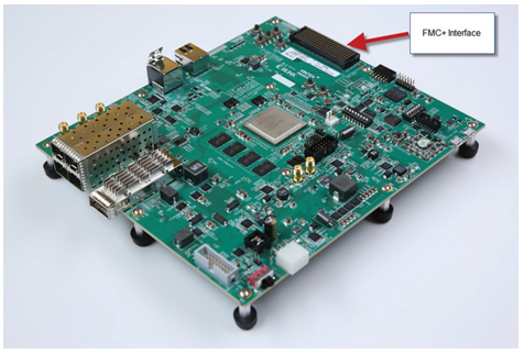
Figure 3 - Xilinx KCU114 Demo Board with FMC+
1. ExtendedOperatingTemperatureRange: Greensaver batteries are able to operate under the harshest environments from-40℃-+60℃temperatures
2. Maintains High Capacity Under Low Temperatures: Greensaver Batteries are able to hold 80-85% of their total capacity under-10℃temperatures.
3. Optimized for High Current Discharge: Greensaver batteries have low resistance, and are superior at discharging large currents.
4. High Charge Acceptance Ability: With low internal resistance, Greensaver batteries have high charge efficiency and have fast charging ability.
5. LongBatteryLife: Without electrolyte stratification using patented electrolyte, Greensaver batteries have cycle life more than 800 cycles.
6. Safety and Reliability: Maintenance free valve regulated design, no acid spilling and no release of acid vapors.
7. Low Internal Resistance: Overheating do not generate easily during charging, This will prolong the service life of the batteries. The ability to receive little current is enhanced.
8. Minimal Self Discharging: Using high purity materials ensure low self-discharge. Batteries retain normal usage one year after fully charging.
9. Environment Friendly: The sulfuric acid in the electrolyte is dispersed within the three dimensional gel networks. Greensaver batteries have less evaporation of acid fume, and do less harm to the environment.
Electric Bicycle Silicon Battery
MAIN NEW ENERGY CO.,LTD , https://www.greensaver-battery.com