Phase compensation of the op amp
In order for the op amp to work properly, a phase compensation capacitor is often added between the input and output in the circuit.
1, about the compensation capacitor
There are some theoretical calculations, but as far as the design is mature, most people rely on the previous debugging experience. Generally, the value of the capacitor should take into account the frequency response of the system (simplifiedly, the larger the capacitance is added, The narrower the bandwidth, then the oscillation problem; if you have to calculate, you can look at the distribution capacitance of the input of the op amp. For example, the negative feedback amplifier circuit is to ensure the resistance of the input and the distributed capacitance. Product = the product of the feedback resistor and the capacitance you want to add. . . . .
2, two works
1. Change the phase shift of the feedback network to compensate for the phase lag of the op amp
2. Compensate for the effect of the capacitance at the input of the op amp (in fact, the final phase is compensated...)
Because the op amps we use are not ideal.
Generally, the operational amplifier used in practice has a corresponding phase shift effect on a signal of a certain frequency. Such feedback of the signal to the input terminal will make the amplifier circuit unstable or even oscillate. For this reason, a corresponding capacitor must be added to compensate the phase. The compensation capacitor is usually built in the op amp. Of course, it can be added to the circuit if necessary. The value depends on the signal frequency and circuit characteristics.
Op amp input compensation capacitor
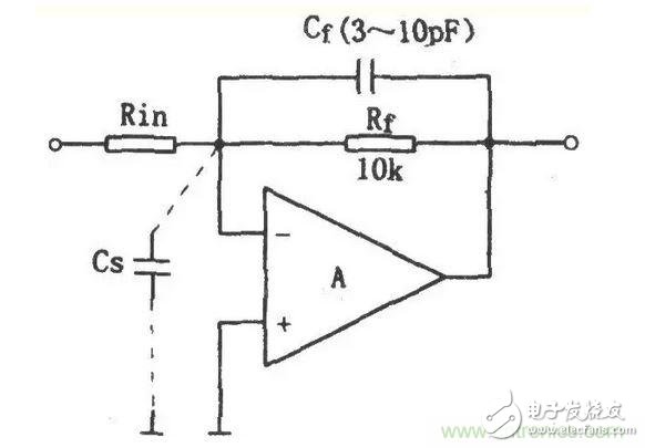
The input parasitic capacitance Cs of a generally linearly operating amplifier (ie, an amplifying circuit that introduces a negative feedback) affects the stability of the circuit. The compensation measures are shown in the figure. The input end of the amplifier generally has a parasitic capacitance Cs of about several picofarads. This capacitor includes the input capacitance of the op amp and the distributed capacitance of the wiring. It forms a hysteresis network with the feedback resistor Rf, causing the output voltage to lag in phase, when the frequency of the input signal is very high. When high, the bypass of Cs degrades the high frequency response of the amplifier, and the upper frequency of the band is approximately:
Ωh=1/(2πRfCs)
If the resistance of Rf is large, the upper limit frequency of the amplifier will be seriously degraded, and the additional lag phase introduced by Cs and Rf may cause parasitic oscillation, which may cause serious stability problems. A simple solution to this is to reduce the resistance of Rf so that ωh is higher than the frequency range of the actual application, but this method will reduce the voltage amplification of the op amp (due to Av = -Rf / Rin). In order to keep the voltage amplification factor of the amplifying circuit high, a more general method is to connect a compensation capacitor Cf on the Rf to make the RinCf network and the RfCs network form phase compensation. RinCf will cause the output voltage phase to lead. Since the value of Cs cannot be accurately known, the phase lead and hysteresis cannot be fully compensated. Generally, the variable capacitor Cf is used to minimize the additional phase shift by experiment and adjustment of Cf. If Rf = 10 kΩ, the typical value of Cf is 3 to 10 pF. For a voltage follower, the Cf value can be slightly larger.
Op amp output capacitor compensation
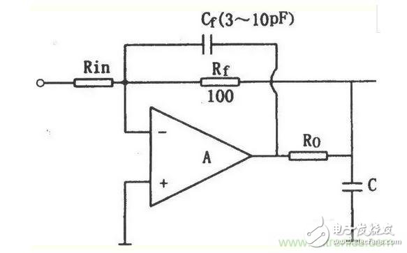
For many integrated operational amplifier circuits, if the value of the output load capacitance CL is much larger than 100pF, since the output capacitance (including parasitic capacitance) and the output resistance will cause additional phase shift, the accumulation of this additional phase shift may generate parasitic oscillations, making the amplifier The work is seriously unstable. The solution to this problem is to connect a resistor Ro in series with the output of the op amp to isolate the load capacitor CL from the amplifier circuit. As shown in the figure, connect the feedback resistor Rf to the rear of Ro. This compensates for DC attenuation and adds feedback. Capacitor Cf will reduce the high-frequency closed-loop voltage amplification factor. The selection method of Cf is: make the amplifier circuit Xcf ≤ Rf/10 at unity gain frequency fT, and Xf = l / (2πfTCf), in general, Ro = 50 to 200 Ω, Cf is about 3 to 10 pF.
In addition to the above-mentioned unstable factors, there are other unstable factors, some of which come from the integrated chip itself. Some are derived from system circuits (such as the coupling problem of the internal impedance of the power supply). Sometimes it is difficult to solve the instability problem by using many methods, but the problem can be solved by using the appropriate compensation method. E.g. When the amplifier does not require a too wide frequency band and the optimum slew rate, the overcompensation method for the integrated op amp will achieve good results, such as increasing the compensation capacitor by a factor of 9 or the multiple required to achieve stability, for μA301 For an op amp, the effect is generally better.
Maskking(Shenzhen) Technology CO., LTD , https://www.szelectroniccigarette.com