Through Silicon Via (TSV) technology is a high-density packaging technology that is gradually replacing the current mature wire bonding technology and is considered to be the fourth generation packaging technology. TSV technology achieves vertical electrical interconnection of through-silicon vias by filling conductive materials such as copper, tungsten, and polysilicon. Through-silicon via technology can reduce interconnect length through vertical interconnects, reduce signal delay, reduce capacitance/inductance, achieve low power consumption between chips, high-speed communication, increase bandwidth, and achieve miniaturization of device integration. The 3D package based on TSV technology has the following advantages:
1) Better electrical interconnection performance,
2) wider bandwidth,
3) higher interconnect density,
4) lower power consumption,
5) smaller size,
6) Lighter quality.
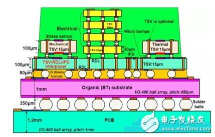
Figure 1 Schematic diagram of future TSV package devices
The TSV process mainly includes deep silicon etching to form micropores, deposition of insulating/barrier/seed layer, deep hole filling, chemical mechanical polishing, thinning, preparation of pad and preparation of redistribution lines. The main process consists of several parts:
(1) formation of through holes;
(2) deposition of an insulating layer, a barrier layer and a seed layer;
(3) copper filling (electroplating), removal and redistribution lead (RDL) plating;
(4) Wafer thinning;
(5) Wafer/chip alignment, bonding and slicing.
TSV deep hole filling technology is a key technology of 3D integration, and it is also a difficult link. TSV filling effect is directly related to the reliability and yield of integrated technology, while high reliability and yield are practical for 3D TSV stack integration. Chemistry is crucial. Another aspect is to maintain good integrity during substrate thinning and to avoid crack propagation is another difficulty in the TSV process. At present, the main technical difficulties are divided into several aspects:
(1) etching of through holes - laser etching, deep reactive ion etching;
(2) Filling of through holes - materials (polysilicon, copper, tungsten and polymer conductors, etc.) and technology (electroplating, chemical vapor deposition, polymer coating, etc.);
(3) Process flow - first through hole or back through hole technology;
(4) Stacked form - wafer to wafer, chip to wafer or chip to chip;
(5) Bonding mode - direct Cu-Cu bonding, bonding, direct fusion, welding and mixing;
(6) Processing of ultra-thin wafers - whether or not to use carriers.
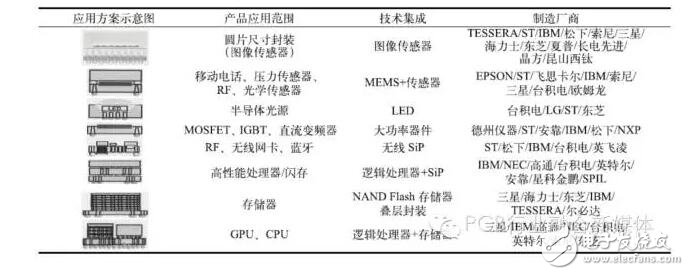
At present, 3D-TSV system packaging technology is mainly applied to image sensors, adapter boards, memories, logic processors + memories, mobile phone RF modules, MEMS wafer level three-dimensional packaging.
Table 1 TSV three-dimensional packaging application field
After several years of research and development, it has formed a 3D package silicon-based adapter board with high yield, different aspect ratio structure, high density microvia, and high conduction rate, which can be widely used in the three-dimensional packaging field of RF, memory and other chips.
In view of the technical difficulties in the current TSV process, the composite etching technology is used to realize the micro-hole preparation of the high aspect ratio structure, the unique thin film deposition technology is used to construct the uniform and dense insulating layer, and the metal interconnection microchannel filling is performed by the precision electrodeposition technology. The shape of the interconnected microchannels can be effectively controlled to effectively solve the heat dissipation problem in high-density interconnects. Through the comprehensive thinning technology, the ultra-thin TSV adapter board can be effectively processed to solve the problem that the thinning process is easy to crack in the TSV three-dimensional package, and the industrialization of the TSV three-dimensional package is achieved.
Shanghai Central Core TSV main technical parameters
Aspect ratio: 1:1-20:1
Pore ​​size: 50 -200μm
Silicon substrate thickness: 200 -300μm
Filling status: solid hole, side hole
Filling material: copper, tungsten
Through hole yield: "95%
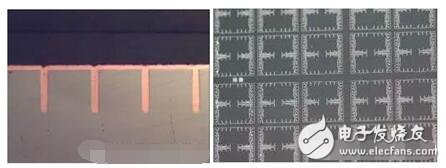
Figure 2 TSV package structure
This have Xbox one wires and wirelss gaming controller For Xbox one console, many are our private model with compectitive price and high qualtiy,all controller we got CE,FCC, RoHS , we also can do others certificates for you. and we customize your logo ,package , carton ect.we accept OEM/ODM,welcome your inquiry.
we are good partner you can trust.
Both Xbox one wired and wireless we can do transparent for you !


Xbox One Controller,Wired Controller Gamepad,Wired Joystick For Xbox One,Xbox One Console Wired
Shenzhen GEME electronics Co,.Ltd , https://www.gemesz.com