In the development process of the home fire alarm system project, the author needs to frequently access the operating data with the slave MCU when performing master-slave communication and slave self-task processing. In the past, the traditional method was to externally EEPROM on the MCU or to divide some memory cells inside the MCU to access the running data. The disadvantage of these two methods is that the external EEPROM needs to increase the read and write interface between the MCU and the EEPROM, which increases the load on the MCU, slows down the data read and write speed, and increases the power consumption; Dividing the storage unit reduces the storage space of the program code, and the operations of reading and writing, erasing, etc. of the storage space are troublesome, and it is also very careful to prevent the useful program code from being erased.
Renesas RL78 series MCU embedded 2KB DATA FLASH, eliminating the need for users to separately expand data FLASH. The RL78 series MCU also supports BGO operation, and the program instructions can still be executed normally during DATA FLASH reading and writing. Its write operation life on DATA FLASH memory cells is more than 1 million times, which is very suitable for applications that require frequent access to data.
Unlike some semiconductor manufacturers' control chips, Renesas does not directly open the DATA FLASH read and write operations to the user, but provides a software interface called PFDL (Pico Data Flash Library). To achieve the operation of the flash system. When the user uses it, he only needs to call the corresponding library function to perform operations such as reading, writing, verifying, and erasing the DATA FLASH without having to care about the specific implementation of the underlying driver function. This greatly facilitates the design of the user program and shortens the development cycle.
1) DATA FLASH structure and PFDL
The storage junction of the RL78 is shown in Figure 1. The physical address of the Data Flash memory is F1000H-F17FFH, which is divided into two BLOCK areas, each of which is 1 KB in total, 2 KB in total.
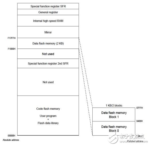
Figure 1: Storage structure of Renesas RL78 series MCU
The PFDL consists of the library files shown in Table 1.
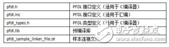
Table 1: PFDL library files
2) Data Flash storage structure and usage
First of all, it is necessary to explain several problems of the RL78 series MCU on DATA FLASH operation. The RL78 series DATA FLASH erase operation can only be in BLOCK unit and does not support single word or single byte erase. Therefore, when a data with a length of several bytes is to be written to the DATA FLASH, it is impossible to write the data to the storage unit corresponding to the fixed physical address each time, but must be written in the new empty storage unit. . This means that users must have addressing capabilities when designing the DATA FLASH memory structure.
RL78 series DATA FLASH can only have one BLOCK active at the same time, which is valid. At this time, another BLOCK is inaccessible and invalid. Habitually, we often refer to a BLOCK of DATA FLASH as a page. When a valid page is filled with data, if you want to continue writing data, you can only write it on the next page, and you need to add the previous one. The other data items useful in the page are copied to the next page, and the next page is marked as the current valid page, and the previous page is marked as an invalid page, that is, there must be a DATA FLASH page mark and a page guide mechanism.
To this end, the author divides the entire DATA FLASH into two pages (each BLOCK naturally forms one page, two pages alternately use), and the starting address of each page serves as a page marking unit, as shown in Table 2. The tag unit should be read to confirm the currently valid page before each DATA FLASH operation.
Table 2: Page Markers
Standard Recovery Stud Diode are mainly used for rectifying and switching
It has positive pressure reduction (0.4v -- 1.0v), short reverse recovery time (2-10ns nanosecond), large reverse leakage current, low pressure resistance, generally lower than 150V, and is used in low voltage situations.
Diodes are electronic devices that have two electrodes that allow only a single current to flow in a single direction.Varicap bond (bond) is an electronic adjustable capacitor.Most diodes have a current orientation that we call reading "rectifier".The most common function of a diode is to allow only the current to pass in one direction (called forward bias) and to block in the opposite direction (called reverse bias).
Standard Recovery Stud Diode,Standard Recovery Diode,400V Standard Recovery Diode,Stud Diode
YANGZHOU POSITIONING TECH CO., LTD. , https://www.yzpst.com