It is important to open the switch on the low side because there is almost no loss in this transition phase, ie "lossless opening". After the high side switch is turned off, the inductor current drives the switch node voltage without loss of ground. The best time to turn on the low side switch is at the end of the transition. If the body diode is briefly conducting before the low side is turned on, it does not matter because it does not cause reverse recovery losses. The excess current at the junction is fully dissipated before the next switch transition. However, if the current is still present in the body diode for a long time, there will be excessive conduction loss. The high-side FET turn-on timing is the most important transition. Because of the cross-conduction with the low-side FET, premature turn-on causes shoot-through loss; too late turn-on leads to increased conduction losses, and excess current is injected into the low-side FET body diode (which must be recovered). In either case, efficiency will be reduced.
To illustrate the timing relationship between efficiency and drive signals, I built some power supplies with adjustable delays for the driver signals. After that, I compared the efficiency and delay time and studied the relationship between them. Figures 1A-1C show the results.
Figure 1A shows what happens when the high side FET is turned on before the low side FET is fully turned off. There is a significantly larger Miller region in the low side gate drive with its low side FET and high side FET turned on simultaneously, producing a shoot-through current in the power stage. When the low side FET is finally turned off, there is an additional voltage overshoot at the switch node. In FIG. 1B , the high side FET is turned on after the low side FET is turned off and a current is formed in the body diode. When the high side FET is turned on, it restores the body diode and there is a current spike that causes the switching node voltage to ring. However, this phenomenon is not obvious because the reverse recovery time (12 nS) of the MOSFET body diode used is extremely short. The slower the body diode speed, the more pronounced the ringing. Figure 1C has the highest power efficiency. Before the high side switch is turned on, the low side gate voltage drops to near the ground voltage. The high side is turned on before the lower body diode conducts, and the switching node ringing is minimized.

Figure 1A Advanced high-side timing produces shoot-through current

Figure 1B High-voltage side drive delay when the body diode is conductive

Figure 1C Optimal Timing Brings Higher Efficiency and Lower Stress
Figure 2 shows the efficiency curves for a 12 volt to 1 volt / 15 amp, 300 kHz power stage for different gate drive timings. The left side of the scale indicates that the high side switch is turned on early, as shown in Figure 1A . The right side represents a delayed high side gate drive ( Figure 1B ). On the left, the efficiency drops sharply due to the through current loss of the power stage. On the right, efficiency gradually decreases.
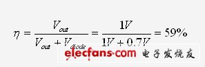
There are two reasons for the gradual decline in efficiency: conduction loss and reverse recovery loss from the low-side FET body diode. During conduction of the body diode, the body diode voltage drops by approximately 0.7 volts. Equation 1 shows the maximum power efficiency during conduction of the body diode, which is roughly as follows:
 Equation 1
 If the body diode is conductive for 50ns in 3us, it can have an effect on the overall efficiency of about 1.2%. For this power stage, the reverse recovery loss is negligible due to the use of a 12 nS short reverse recovery time MOSFET.

Figure 2 driver timing can greatly affect efficiency
In summary, the correct gate drive signal timing in a synchronous buck regulator is critical to maximizing efficiency. This timing minimizes the conduction time of the low-side FET body diode. High-side FET turn-on is the most critical transition phase, and should avoid turning on the high-side FET before the low-side side is fully turned off. Doing so minimizes switching losses and reduces voltage ringing during the transition.
Warning Lights are generally used to maintain road safety. They are usually used in police cars, engineering vehicles, fire engines, ambulances, maintenance management vehicles, road maintenance vehicles, tractors, emergency A/S vehicles, mechanical equipment, etc., machinery, electricity, Control signals interlocking in electrical control circuits such as machine tools, chemicals, telecommunications, ships, and metallurgy.
For Warning Lights,we have our own research and development team,we are always committed to providing the best service to all clients,in our company,the Warning Light are mainly divided into these series:
BPT5 Bulb/LED Tower Light
BPTL5 Bulb/LED Tower Light
BPT7Z Bulb/LED Tower Light
B-2071 Mini Warning Light
B-1101 LED Warning Light
B-TYN Solar LED Warning Light
B-1101ROG Multiple Colors LED Warning Light
MS190 290 390 Sirens
Buzzers
Warning Lights
Warning Lights,Tower Light,Warning Lamp,LED Tower Light
Ningbo Bond Industrial Electric Co., Ltd. , https://www.bondelectro.com