1 The basic principle of the touch screen
This article refers to the address: http://
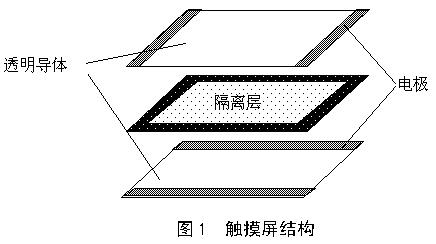
The working part of a typical touch screen generally consists of three parts, as shown in Figure 1: two transparent resistive conductor layers, an isolation layer between the two conductors, and an electrode. The resistive conductor layer is made of a resistive material such as indium tin oxide (ITO) coated on the substrate, the upper substrate is made of plastic, and the lower layer is made of glass. The barrier layer is a viscous insulating liquid material such as a mylar film. The electrode is made of a material with excellent electrical conductivity (such as silver powder ink), and its electrical conductivity is about 1000 times that of ITO.
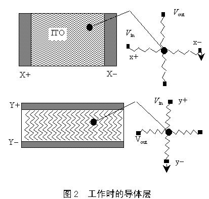
  
When the touch screen is working, the upper and lower conductor layers are equivalent to the resistor network, as shown in Figure 2. When a layer of electrodes is applied with a voltage, a voltage gradient is formed across the network. If there is an external force that causes the upper and lower layers to contact at a certain point, the voltage at the contact point can be measured at another layer where the electrode is not applied with voltage, thereby knowing the coordinates at the contact point. For example, when a voltage is applied to the top electrode (X+, X-), a voltage gradient is formed on the top conductor layer. When an external force is applied to make the upper and lower layers contact at a certain point, the voltage at the contact point can be measured at the bottom layer. Then, based on the distance relationship between the voltage and the electrode (X+), the X coordinate of the place is known. Then, the voltage is switched to the bottom electrode (Y+, Y-), and the voltage at the contact point is measured at the top layer to know the Y coordinate.
2 touch screen control implementation
In many PDA applications, the touch screen is used as an input device, and the control of the touch screen also has a special chip. Obviously, the touch screen control chip has to do two things: one is to complete the switching of the electrode voltage; the other is to collect the voltage value at the contact point (ie A/D). This article takes the chip ADS7843 produced by BB (Burr-Brown) as an example to introduce the realization of touch screen control.
2.1 Basic Features and Typical Applications of ADS7843
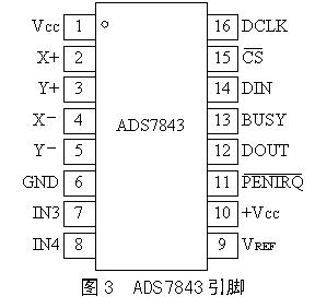
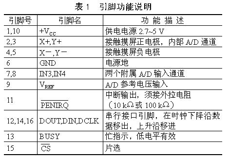
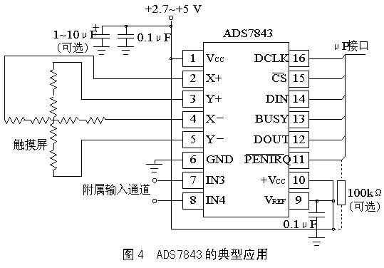
The ADS7843 is a serial interface chip with a built-in 12-bit analog-to-digital conversion and low on-resistance analog switch. The supply voltage is 2.7~5 V, the reference voltage VREF is 1 V~+VCC, the input range of the conversion voltage is 0~VREF, and the maximum conversion rate is 125 kHz. The pin configuration of the ADS7843 is shown in Figure 3. Table 1 shows the pin function description, and Figure 4 shows the typical application.
2.2 ADS7843 internal structure and reference voltage mode selection
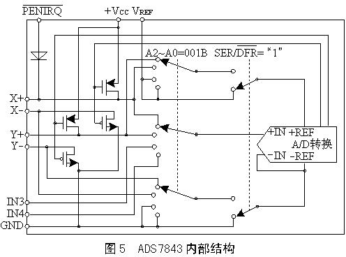
The ADS7843 is able to control the touch screen because its internal structure makes it easy to switch the electrode voltage and enable fast A/D conversion. Figure 5 shows its internal structure. A2~A0 and SER/ are the control bits in the control register for switching and reference voltage selection.
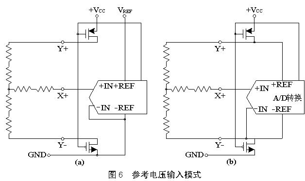
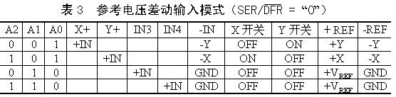
The ADS7843 supports two reference voltage input modes: one with a fixed reference voltage of VREF and the other with a differential mode with a reference voltage from the drive electrode. These two modes are shown in Figures 6(a) and (b), respectively. Using the differential mode of Figure 6(b) eliminates the effects of the switch-on voltage drop. Table 2 and Table 3 show the internal switch conditions corresponding to the two reference voltage input modes.
  
  
2.3 ADS7843 control word and data transmission format
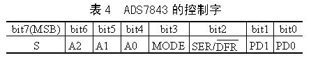
The control words of the ADS7843 are listed in Table 4, where S is the data transmission start flag and this bit must be "1". A2~A0 for channel selection (see Tables 2 and 3).
MODE is used to select the accuracy of A/D conversion. "1" selects 8 bits and "0" selects 12 bits.
Input mode for SER/select reference voltage (see Tables 2 and 3). PD1 and PD0 select the power saving mode:
The "00" power saving mode allows power to be lost between two A/D conversions, and the interrupt is allowed;
"01" is the same as "00", but it is not allowed to interrupt;
"10" reserved;
"11" prohibits the power saving mode.
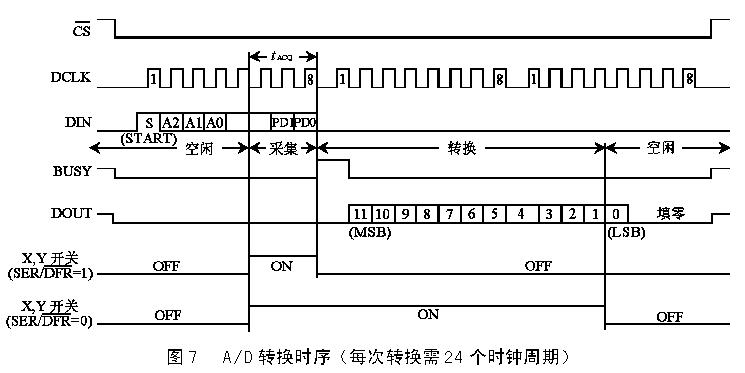
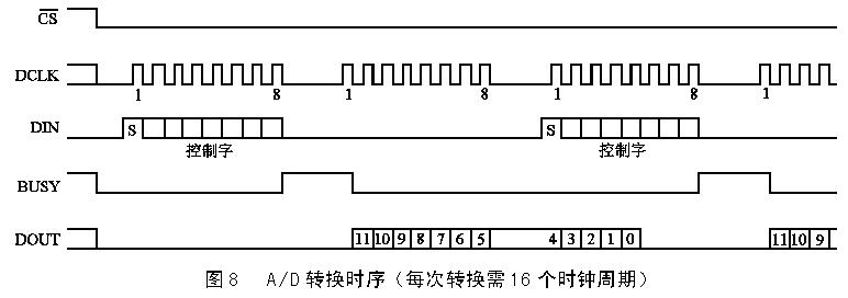
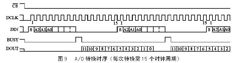
In order to complete the electrode voltage switching and A/D conversion, the control word needs to be sent to the ADS7843 through the serial port. After the conversion is completed, the voltage conversion value is read through the serial port. A standard one conversion takes 24 clock cycles, as shown in Figure 7. Since the serial port supports bidirectional simultaneous transmission and can overlap between one reading and the next transmission of the control word, the slew rate can be increased to 16 clock cycles each time, as shown in FIG. If the CPU can generate 15 CLKs (such as FPGAs and ASICs), the conversion rate can be increased to 15 clock cycles each time, as shown in Figure 9.
  
 2.4 A/D conversion timing programming
A typical application of the ADS7843 is shown in Figure 4. Assume that the μP interface is connected to P1.3~P1.7 of 51 MCU. Now, taking 24 clock cycles for one conversion as an example, the program design of A/D conversion timing is introduced.
; A / D interface control line
DCLK BIT P1.3
CS BIT P1.4
DIN BIT P1.5
BUSY BIT P1.6
DOUT BIT P1.7
; A/D channel select command word and working register
CHX EQU 094H; channel X+ selection control word
CHY EQU 0D4H; channel Y+ selection control word
CH3 EQU 0A4H
CH4 EQU 0E4H
AD_CH EQU 35H ; channel select register
AD_RESULTH EQU 36H ; store 12 bit A/D value
AD_RESULTL EQU 37H
; Store the A/D value of channel CHX+
CHXAdResultH EQU 38H
CHXAdResultL EQU 39H
; Store the A/D value of channel CHY+
CHYAdResultH EQU 3AH
CHYAdResultL EQU 3BH
; Acquisition channel CHX+ block (CHXAD)
CHXAD: MOV AD_CH, #CHX
LCALL AD_RUN
MOV CHXAdResultH, AD_RESULTH
MOV CHXAdResultL, AD_RESULTL
RET
; Acquisition channel CHY+ block (CHYAD)
CHYAD: MOV AD_CH, #CHY
LCALL AD_RUN
MOV CHYAdResultH, AD_RESULTH
MOV CHYAdResultL, AD_RESULTL
RET
; A / D conversion subroutine (AD_RUN)
; Input: AD_CH-mode and channel selection command word
; Output: AD_RESULTH, L; 12 bit A/D conversion value
; Use: R2 ; Auxiliary working register
AD_RUN:
CLR CS ; chip allowed
CLR DCLK
MOV R2, #8; write 8 bit command word first
MOV A, AD_CH
AD_LOOP:
MOV C, ACC.7
MOV DIN, C; clock rising edge latch DIN
SETB DCLK ; start sending command words
CLR DCLK; clock pulse, a total of 24
RL A
DJNZ R2, AD_LOOP
NOP
NOP
NOP
NOP
ADW0: JNB BUSY, AD_WAIT; waiting for conversion to complete
SJMP ADW1
AD_WAIT:
LCALL WATCHDOG
NOP
SJMP ADW0
CLR DIN
ADW1: MOV R2, #12 ; start reading 12bit results
SETB DCLK
CLR DCLK
AD_READ:
SETB DCLK
CLR DCLK ; read with the falling edge of the clock
MOV A, AD_RESULTL
MOV C, DOUT
RLC A
MOV AD_RESULTL, A
MOV A, AD_RESULTH
RLC A
MOV AD_RESULTH, A
DJNZ R2, AD_READ
MOV R2, #4; Finally, 4 clocks that are useless
IGNORE:
SETB DCLK
CLR DCLK
DJNZ R2, IGNORE
SETB CS; banned chip
ANL AD_RESULTH, #0FH ; shield high 4 bit
RET
2.5 A/D conversion result data format
The ADS7843 conversion result is in binary format. It should be noted that the reference voltage is different in the two input modes when formula calculation is performed. Moreover, if the 8-bit conversion precision is selected, 1LSB=VREF/256, the conversion completion time can be advanced by 4 clock cycles, and the serial clock rate can be doubled.
Conclusion
In many embedded systems, the CPU provides specialized modules to support the input of the LCD and touch screen, making the interface very simple. For example, MOTOROLA's MC68VZ328 (called Dragon Ball) provides dedicated pins to support 8-bit and 4-bit LCD displays. Support for touch screens is also easily accomplished with SPI2 via the ADS7843.
Why the Glass wall curtain led display can lead the fashion of outdoor media?
The LED Glass curtain display appeared as an sudden emergence on the outdoor media market.
With the advantages of encapsulation technology, high brightness, wide viewing angle, adjustable screen area and easy installation, The transparent LED Glass Display has gradually replaced the traditional billboards, light boxed, etc., And become the high-profile new force for outdoor advertising media. At the same time, a small pitch is applicable to the Glass Wall Led Screen and led glass screen for window. There`re various types of led display products suitable for glass wall and glass window, such as Transparent led display and Led Strip Curtain screen. As if, indoor and outdoor led curtain wall display has become a leading industry for led display market
Led Glass Display,Led Display For Glass Window,Outdoor Transparent Led Display,Glass Wall Led Screen
Shenzhen Priva Tech Co., Ltd. , https://www.privaled.com