1. Continuous technological innovation Currently, more than 80% of polysilicon production technologies are modified Siemens method, and there are two prominent representatives: one is the non-closed process represented by German WACKER; the other is the adoption of Jiangsu Zhongneng, a subsidiary of GCL-Poly. The modified Siemens process closed loop production process. The advantage of technological innovation and process optimization is that it can comprehensively improve the indicators in production. For example, taking the energy consumption index of GCL as an example, the integrated power consumption is between 70 and 80 kWh/kg, and the reduction power consumption is 40 kWh/kg. This indicator is far better than the world's advanced level. Dachang integrated power consumption is in the range of 100 to 120 kWh per kilogram. 2. To achieve large-scale operations The history of polysilicon is a history of competition for meat and food. The Chinese polysilicon industry, which has risen in the era of photovoltaics, is also experiencing such a process. Scale management has the concept of a single-line economy. Take GCL as an example. With the expansion of single-line production costs, the production costs will drop by 20% to 50% every year. The production cost of 10,000 tons of single-line production in 2012 can be reduced to 17 US dollars/kg, a 15% decrease from 2011. . Large-scale operations also have concentrated problems. Polysilicon production is a huge system of combined cycle, multi-line joint formation of centralized control, public support, and mutual support to ensure the long-term stable operation of the system security. From the experience of GCL, the configuration of three single production lines can ensure the maximization of scale operations.
3. Reasonable industrial layout In 2012, there were 33 polysilicon companies with a capacity of over 1,000 tons in China, and the project was very fragmented. There were only two tens of thousands of tons, with an average of less than 5,000 tons. The Ministry of Industry and Information Technology's “Entry of Polysilicon Industry†issued in 2011 made provisions for the layout of polysilicon projects. This is because energy costs account for the largest proportion of polysilicon production costs. However, taking energy as the layout is not the only condition. The high-tech characteristics of polysilicon determine the importance of talents and industry support. Moreover, through the systematic application of energy-saving and consumption-reduction technologies, the impact of electricity prices on production costs has been largely absorbed.
4. Play a role in industrial synergy The industry has always been arguing about whether photovoltaics are specialized or whether they are good for the whole industry chain. In fact, in any industry, the only criterion for professionalism or full industrialization is the ability of the company. The first thing to do is to do a good job in this major, first do a special job, then go upstream and downstream. Integration must be a strategy to take the initiative and not be an expedient measure.
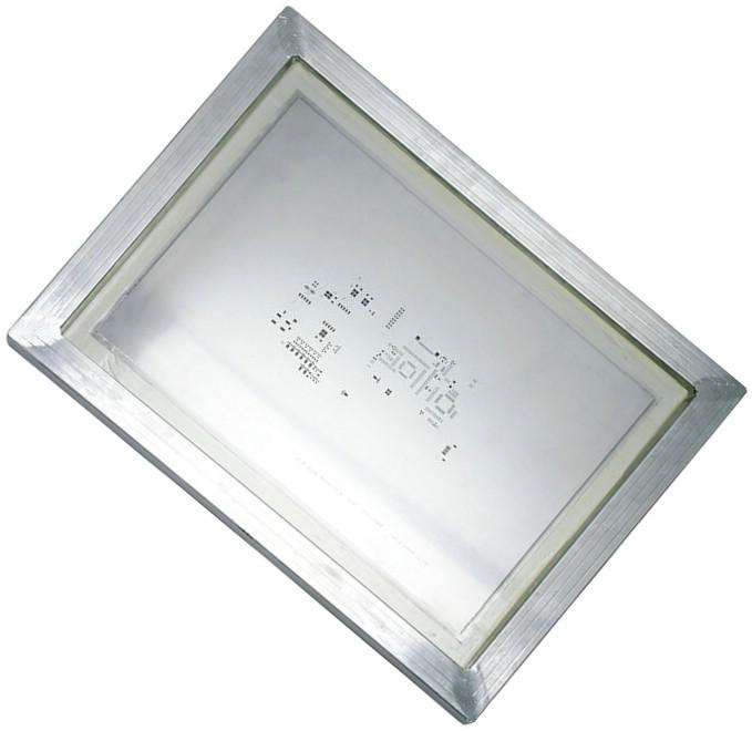
SMT Stencil is made of stainless steel, and used for printing the solder paste on the SMT pads when do PCB Assembly job. Ours SMT stencil is high-precision Laser stencils which is OK for 0.3mm BGA PCB Assembly.
SMT Stencil could be framed SMT stencil and also could be un-framed SMT stencil.
For un-framed SMT stencil, the biggest size is 280mm*380mm and the valid size is 190mm*290mm. And also the size could be customized if required, just ensure the stencil size is bigger than the PCB boards. Normally, un-framed stencil is used for PCB hand assembly or PCB Prototype assembly which is cheap and convenient.
For framed SMT stencil, it has many sizes could be chose and it`s always used for PCB automatic assembly or big quantity PCB assembly. It could be put on the auto solder paste print machine in the automatic SMT line.

SMT Stencil
SMT Stencil,Laser SMT Stencil,PCB SMT Stencil,Stainless SMT Stencil
ZhongFeng Electronic Technology Co., Limited , https://www.dopcba.com